


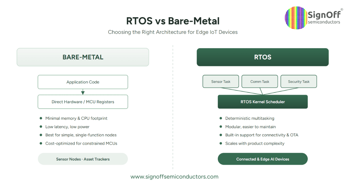
Author – Saraswati Bhat, Software Engineer - I - EmbeddedChoosing Between RTOS and Bare-Metal for Edge IoT Devices: A Guide...
Read More
Blog
26
Feb
2020
ASIC vs FPGA
Before starting the discussion on what is ASIC and what is FPGA, we will first learn about the basics that a VLSI enthusiast should know. Moore’s Law: Moore’s law is the observation that the number of transistors in a dense integrated circuit doubles about every two years.
25
Nov
2019
Introduction to SDC
Before starting the discussion on what is ASIC and what is FPGA, we will first learn about the basics that a VLSI enthusiast should know. Moore’s Law: Moore’s law is the observation that the number of transistors in a dense integrated circuit doubles about every two years.
6
Feb
2019
Gate All Around FET
GAA is somehow similar to FinFETs except the conducting channel is surrounded by gate all around. Thus we get better gate controllability over the channel. The channel shape can be square or any other polygon shape.
5
Feb
2019
Communication Protocols
UART stands for Universal Asynchronous Receiver-Transmitter. It is commonly used in the microcontroller to communicate with the peripheral. An 8-bit serial data coming from the peripheral device is converted into the parallel form using serial to parallel conversion and parallel data coming from the CPU is converted using parallel to serial conversion.
14
Dec
2018
Bulk CMOS
CMOS technology uses both NMOS and PMOS transistors, The transistors are arranged in a structure formed by two complementary networks. Bulk CMOS is a chip built on a standard silicon wafer.
14
Dec
2018
FinFET-2 (Multi-Gate FinFET)
In 1965, Gorden Moore in his paper predicted that how number of transistors in integrated circuit get double in every 18 month. Even though in 1990, a new type of substrate named SOI (Silicon-on-insulator) was introduced which improved the speed and power consumption, the first integrated circuit transistor was fabricated on “Bulk” silicon wafers.
11
Dec
2018
Silicon On Insulator ( SOI )
Silicon on insulator (SOI) refers to the use of a three layered substrate in place of conventional bulk silicon substrates. A thin layer of silicon is placed on top of an insulator such as silicon dioxide (SiO2) also known as a buried oxide layer.
30
Mar
2018
UPF
Power is one of the most concerned factor in the lower node technologies due to sophisticated operation of a system at higher frequencies, complex functionalities, wireless applications and portability. Power dissipation has become one of the critical issues as it results in heating up of the device which in-turn affects the operation of a chip.
28
Mar
2018
Post CTS Optimization
During Clock tree synthesis, buffers or inverters are added in the clock nets to achieve minimum Insertion delay and Skew, while meeting the clock DRV’s. Various optimizations are performed during CTS such as CCDO (Concurrent Clock and Data Optimization) and CTO (Clock Tree Optimization) .
28
Feb
2018
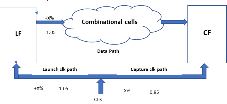
STA-1
What is STA ? Static timing analysis is one of the techniques used to verify the timing of a digital design. STA is static since the analysis of the design is carried out statically and does not depend upon the data values being applied at the input pins of the design.
Customers
Partners
Our Blog
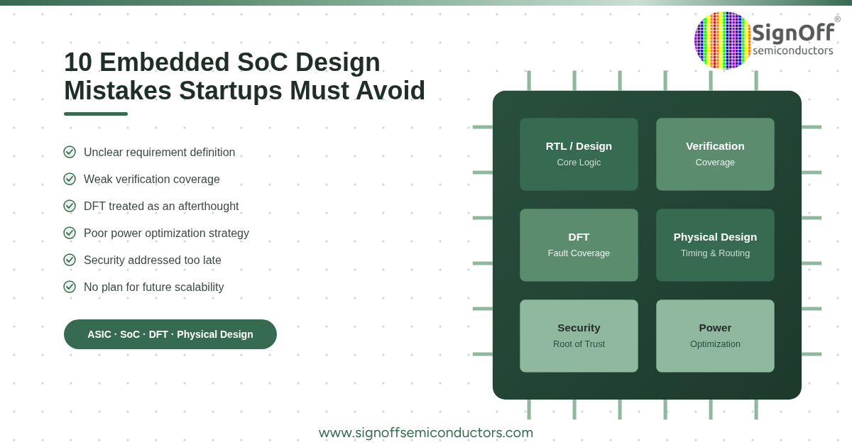
Embedded SoC Design Mistakes Startups Must Avoid
Author – Saraswati Bhat, Software Engineer - I - Embedded Embedded SoC Design Mistakes Startups Must Avoid The race to...
Read More
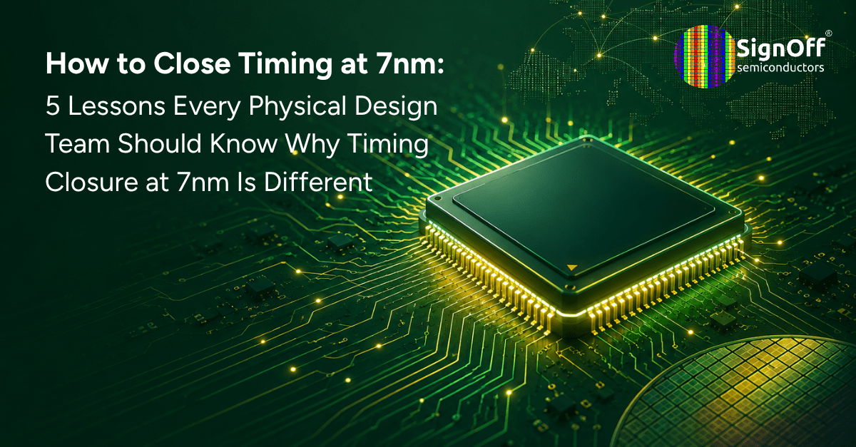
How to Close Timing at 7nm: 5 Lessons Every Physical Design Team Should Know Why Timing Closure at 7nm Is Different
Author - Challa Krishnachaitanya Reddy With 20+ years in Design has worked on tapeouts at sub-5nm How to Close Timing...
Read More

Why LVS Debugging Breaks at 2nm: The Hidden Complexity of GAAFET Verification
Author - Challa Krishnachaitanya Reddy With 20+ years in Design has worked on tapeouts at sub-5nmWhy LVS Debugging Breaks at...
Read More
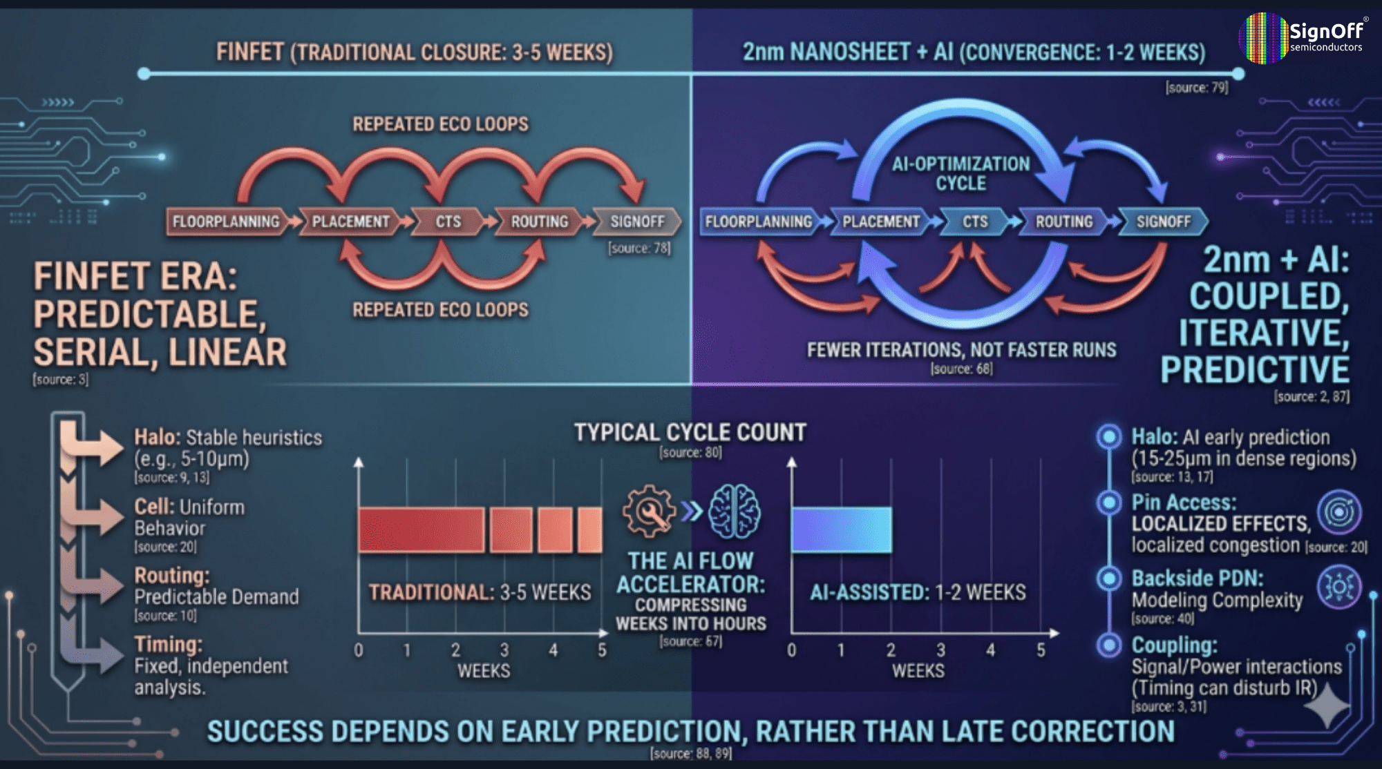
Nanosheet-Aware P&R vs FinFET Flows: Why AI Defines Success at 2nm
Author - Challa Krishnachaitanya Reddy With 20+ years in Design has worked on tapeouts at sub-5nm VLSI Design at...
Read More
Power Optimization at 2nm in 2026
Power Optimization at 2nm in 2026: How N2P and 20A Enable Sub-8% Leakage As the semiconductor industry transitions into the...
Read More

AI Revolution in Semiconductors | Compute, Memory & Edge Growth
The AI Revolution in Semiconductors: How Industry Trends Are Driving Growth Across Compute, Memory, and EdgeInterest in AI hardware is...
Read More
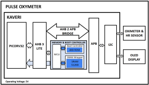
Empowering Healthcare Devices with SignOff’s ASIC SoC: Kaveri
Empowering Healthcare Devices with SignOff’s ASIC SoC: Kaveri The surge in demand for portable healthcare products has accelerated the need...
Read More

Making a Difference: CSR Initiatives by Signoff Semiconductors
Making a Difference: CSR Initiatives by Signoff Semiconductors Introduction Creating a strong social impact has always been one of the...
Read More
OCV, AOCV, and POCV
OCV, AOCV, and POCV In OCV, a fixed delay factor is applied to the delay of all the cells present...
Read More
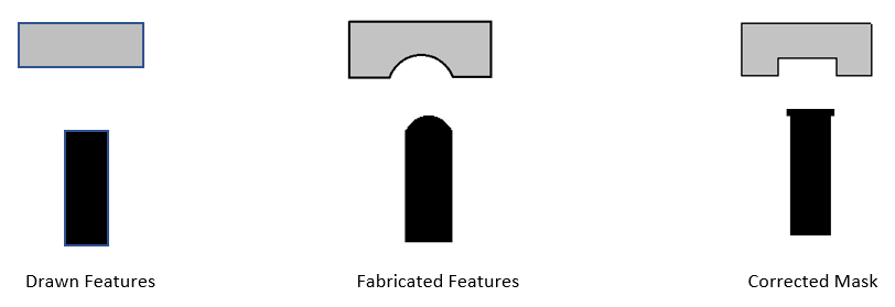
Optical Proximity Correction (OPC)
Introduction Optical Proximity Correction OPC is a resolution enhancement technique based on optical lithography. It is used in sub-wavelength lithography...
Read More
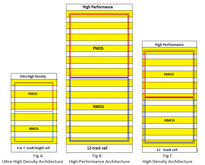
Layout Blog: Standard Cells
Layout Blog: Standard Cells Multiple Architectures Standard-cell library offers multiple architecture for best optimisation in performance, power, and area requirements...
Read More
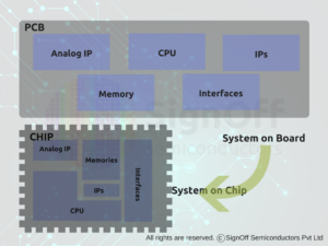
IC Design & Flow Overview
IC Design & Flow Overview INTRODUCTION:Integrated circuits (ICs) have revolutionized the world as we know it. They power the devices...
Read More
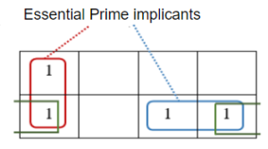
Boolean Expressions-2
We hope you had a good understanding of Boolean Expressions which is available @ Boolean Expressions. In this blog, we...
Read More
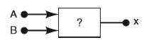
Logic Gates
We hope you had a good understanding of Number Systems which is available @ Number Systems. For building hardware, we...
Read More
Number Systems
To start with VLSI skill development, we need to enhance our frontend skills. check the ASIC flow at ASICvsFPGA, which...
Read More

India Location
Bangalore, India (Registered Office)
1st and 2nd Floor, 228, 6th A Main Rd, 2nd A Block, HRBR Layout, Kalyan Nagar, Bengaluru, Karnataka 560043
CIN : U72200KA2015PTC084617
1st and 2nd Floor, 228, 6th A Main Rd, 2nd A Block, HRBR Layout, Kalyan Nagar, Bengaluru, Karnataka 560043
CIN : U72200KA2015PTC084617
Hyderabad, India
Trendz JR Plot No: 23 &24, 1st Floor, Vittal Rao Nagar, Gafoornagar, Telangana-500081, India.
Trendz JR Plot No: 23 &24, 1st Floor, Vittal Rao Nagar, Gafoornagar, Telangana-500081, India.
Global Locations
San Jose, USA
6469 Almaden Expy Ste 80 #438 San Jose, CA 95120
6469 Almaden Expy Ste 80 #438 San Jose, CA 95120
Canada
Signoff Semiconductors Inc
7725 Markham Road Suite 1007 Markham, ON L3S 3J9 Canada
Signoff Semiconductors Inc
7725 Markham Road Suite 1007 Markham, ON L3S 3J9 Canada
China
Floor 1, Section 1, Pioneer Building, No.7 Kaituo Road, Shangdi Information Industry Base, Haidian Dist., Beijing
Floor 1, Section 1, Pioneer Building, No.7 Kaituo Road, Shangdi Information Industry Base, Haidian Dist., Beijing
Malaysia
SignOff Semiconductors Malaysia SDN BHD,
Penang, Malaysia
SignOff Semiconductors Malaysia SDN BHD,
Penang, Malaysia