


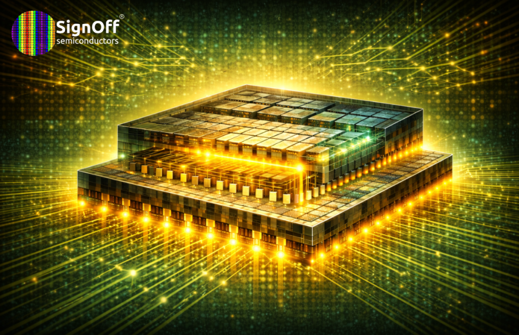
Power Optimization at 2nm in 2026: How N2P and 20A Enable Sub-8% Leakage As the semiconductor industry transitions into the...
Read MoreBlog
24
Feb
2026
Power Optimization at 2nm in 2026
Power Optimization at 2nm in 2026: How N2P and 20A Enable Sub-8% Leakage As the semiconductor industry transitions into the 2nm generation in 2026, power optimization has emerged as one of the most critical constraints in advanced SoC design. Methods that were effective at 7nm and even 5nm such as conventional clock gating or coarse voltage islands no longer deliver acceptable results at
18
Jan
2026
Chiplets Reshaping Semiconductor Design: Cost & Performance
Why Chiplets Are Reshaping Semiconductor Design: A Pragmatic Look at Cost and Performance The Economic Case for Modular Silicon The semiconductor industry is at a crossroads. The discussion on chiplets vs. monolithic, SoCs is now more than just technical. It is changing the way processors are made. Traditional chips are reaching their limits. Wafer costs at advanced nodes exceed $2,000,
17
Dec
2025
AI Revolution in Semiconductors | Compute, Memory & Edge Growth
The AI Revolution in Semiconductors: How Industry Trends Are Driving Growth Across Compute, Memory, and Edge Interest in AI hardware is rising as the semiconductor industry trends towards faster computing and specialised designs. This, in turn, is changing investment focus and market outlook. Organisations across sectors now recognise that competitive advantage increasingly depends on silicon built for intelligence at scale.
10
Nov
2025
Advancing Semiconductor Design: Our Presence at SemIsrael Expo 2025
Advancing Semiconductor Design: Our Presence at SemIsrael Expo 2025 Our Participation at SemIsrael Expo 2025 SignOff Semiconductors will proudly participate in the SemIsrael Expo chip design track on Tuesday, 11 November, 2025 at the Avenue Convention Centre Airport City Israel. This prestigious event is a much-awaited gathering for the global semiconductor industry, connecting technologists and innovators who are shaping next-generation
25
Sep
2025
Empowering Healthcare Devices with SignOff’s ASIC SoC: Kaveri
Empowering Healthcare Devices with SignOff’s ASIC SoC: Kaveri The surge in demand for portable healthcare products has accelerated the need for embedded systems that offer low power consumption, compact size, and precise real-time processing of biomedical data. Pulse oximeters, which measure blood oxygen saturation (SpO₂) and heart rate, exemplify these requirements. This report examines the application of the Kaveri System-on-Chip
13
Feb
2024
Making a Difference: CSR Initiatives by Signoff Semiconductors
Making a Difference: CSR Initiatives by Signoff Semiconductors Introduction Creating a strong social impact has always been one of the major goals for Signoff Semiconductors. As a service-based organization founded on 10th December 2015, we have always believed in giving back to society as much as possible and are dedicated to making a meaningful impact since the initiation of our
6
Dec
2023
OCV, AOCV, and POCV
OCV, AOCV, and POCV Fig1: Derate Factor on Setup Analysis Fig2: Derate Factor on Hold Analysis Issues in OCV: Advance On-Chip Variation (AOCV): Fig3: Bounding box for cell and net distance Distance: If the distance increases, systematic variation will increase, and to mitigate the variation, we need to use a higher derate value. So along with the
27
Oct
2023
Optical Proximity Correction (OPC)
Introduction Optical Proximity Correction OPC is a resolution enhancement technique based on optical lithography. It is used in sub-wavelength lithography to deal with the severe image distortions. These image distortions typically include the: increased corner rounding, line-end shortening and changes in the width when located in isolated or dense environments. This technique helps in improving the imaging resolution. It is
11
Sep
2023
Layout Blog: Standard Cells
Layout Blog: Standard Cells Multiple Architectures Standard-cell library offers multiple architecture for best optimisation in performance, power, and area requirements of Digital designs. High Performance Architecture, a High-Density Architecture for varied customer application requirements. In each requirement (power/performance/area), layout approaches will be different to meet the design specifications. Here, we will covering in more common guidelines. Standard Cell Templates: Based
30
Jan
2023
IC Design & Flow Overview
IC Design & Flow Overview INTRODUCTION:Integrated circuits (ICs) have revolutionized the world as we know it. They power the devices we use every day and have enabled advancements in fields ranging from telecommunications to medicine. But have you ever wondered how these tiny chips, no bigger than a fingernail, are designed and manufactured? The IC design process is a complexRead more
Customers
Partners
Our Blog

AI Revolution in Semiconductors | Compute, Memory & Edge Growth
The AI Revolution in Semiconductors: How Industry Trends Are Driving Growth Across Compute, Memory, and EdgeInterest in AI hardware is...
Read More
Empowering Healthcare Devices with SignOff’s ASIC SoC: Kaveri
Empowering Healthcare Devices with SignOff’s ASIC SoC: Kaveri The surge in demand for portable healthcare products has accelerated the need...
Read More
Making a Difference: CSR Initiatives by Signoff Semiconductors
Making a Difference: CSR Initiatives by Signoff Semiconductors Introduction Creating a strong social impact has always been one of the...
Read More
OCV, AOCV, and POCV
OCV, AOCV, and POCV In OCV, a fixed delay factor is applied to the delay of all the cells present...
Read More
Optical Proximity Correction (OPC)
Introduction Optical Proximity Correction OPC is a resolution enhancement technique based on optical lithography. It is used in sub-wavelength lithography...
Read More
Layout Blog: Standard Cells
Layout Blog: Standard Cells Multiple Architectures Standard-cell library offers multiple architecture for best optimisation in performance, power, and area requirements...
Read More
IC Design & Flow Overview
IC Design & Flow Overview INTRODUCTION:Integrated circuits (ICs) have revolutionized the world as we know it. They power the devices...
Read More
Boolean Expressions-2
We hope you had a good understanding of Boolean Expressions which is available @ Boolean Expressions. In this blog, we...
Read More
Logic Gates
We hope you had a good understanding of Number Systems which is available @ Number Systems. For building hardware, we...
Read More
Number Systems
To start with VLSI skill development, we need to enhance our frontend skills. check the ASIC flow at ASICvsFPGA, which...
Read More
ASIC vs FPGA
Before starting the discussion on what is ASIC and what is FPGA, we will first learn about the basics that...
Read More
Introduction to SDC
Before starting the discussion on what is ASIC and what is FPGA, we will first learn about the basics that...
Read More
Gate All Around FET
GAA is somehow similar to FinFETs except the conducting channel is surrounded by gate all around. Thus we get better...
Read More
Communication Protocols
UART stands for Universal Asynchronous Receiver-Transmitter. It is commonly used in the microcontroller to communicate with the peripheral. An 8-bit...
Read More
India Location
Bangalore, India (Registered Office)
1st and 2nd Floor, 228, 6th A Main Rd, 2nd A Block, HRBR Layout, Kalyan Nagar, Bengaluru, Karnataka 560043
CIN : U72200KA2015PTC084617
1st and 2nd Floor, 228, 6th A Main Rd, 2nd A Block, HRBR Layout, Kalyan Nagar, Bengaluru, Karnataka 560043
CIN : U72200KA2015PTC084617
Hyderabad, India
Trendz JR Plot No: 23 &24, 1st Floor, Vittal Rao Nagar, Gafoornagar, Telangana-500081, India.
Trendz JR Plot No: 23 &24, 1st Floor, Vittal Rao Nagar, Gafoornagar, Telangana-500081, India.
Global Locations
San Jose, USA
6469 Almaden Expy Ste 80 #438 San Jose, CA 95120
6469 Almaden Expy Ste 80 #438 San Jose, CA 95120
Canada
Signoff Semiconductors Inc
7725 Markham Road Suite 1007 Markham, ON L3S 3J9 Canada
Signoff Semiconductors Inc
7725 Markham Road Suite 1007 Markham, ON L3S 3J9 Canada
China
Floor 1, Section 1, Pioneer Building, No.7 Kaituo Road, Shangdi Information Industry Base, Haidian Dist., Beijing
Floor 1, Section 1, Pioneer Building, No.7 Kaituo Road, Shangdi Information Industry Base, Haidian Dist., Beijing
Malaysia
SignOff Semiconductors Malaysia SDN BHD,
Penang, Malaysia
SignOff Semiconductors Malaysia SDN BHD,
Penang, Malaysia