ASIC vs FPGA
Author : Pdv Sai Pavan, Digital Design Engineer, SignOff Semiconductors
Before starting the discussion on what is ASIC and what is FPGA, we will first learn about the basics that a VLSI enthusiast should know.
Moore’s Law: Moore’s law is the observation that the number of transistors in a dense integrated circuit doubles about every two years.
This has been continuously driving the VLSI industry and the results of this law are the latest technological nodes (i.e. 28nm, 14nm, 12nm, 10nm, 7nm, 5nm). The technology node depends on the length of the gate channel. So, if the length of the gate channel is 10nm we call it as 10nm technology node.
Integrated Circuit: An integrated circuit or monolithic integrated circuit (also referred to as an IC, a chip, or a microchip) is a set of electronic circuits on one small flat piece (or “chip”) of semiconductor material that is normally silicon.
We have 3 types of IC’s based on the application. They are ASIC (Application Specific Integrated Circuits), FPGA (Field Programmable Gate Array) and SoC (System On Chip)
ASIC:
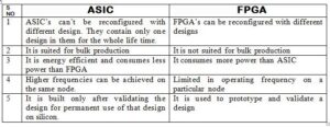
ASIC means Application Specific Integrated Circuit. It is a device that is created for a specific purpose or functionality. They contain only one functionality in them and through the lifetime of the chip, it can perform only that function. For example, CPU in your phone is an ASIC. It is meant to function as a CPU for its whole life. Its logic function cannot be changed to anything else because its digital circuitry is made up of permanently connected gates and flip-flops on silicon. The difference in case of ASIC is that the resultant circuit is permanently drawn into silicon whereas in FPGA the circuit is made by connecting a number of configurable blocks.
FPGA:
FPGA means Field Programmable Gate Array. It can be “field” programmed to work as per the intended design. It means it can work as a microprocessor or graphics card, or even as both at once. The designs running on FPGA’s are generally created using hardware description languages such as VHDL and Verilog. FPGA is made up of number of Configurable Logic Blocks (CLB’s) and are connected with Programmable Interconnects. The CLB’s are primarily made of Look-Up Tables (LUT’s), Multiplexers and Flip-Flops. They can implement complex logic functions. Apart from CLB’s, and routing interconnects, many FPGA’s also contain dedicated hard-silicon blocks for various functions such as Block RAM, DSP Blocks, External Memory Controllers, PLL’s etc. These dedicated hardware blocks are critical in competing with ASIC’s.
SoC:
SoC means System On Chip. It contains one or more microprocessors(cores) or microcontrollers or DSP cores along with all other IP’s(Intellectual Property) such as memory IP, peripheral IPs etc. In other terms, if an ASIC contains one or more processors, it’s called an ASIC.
FPGA Flow:
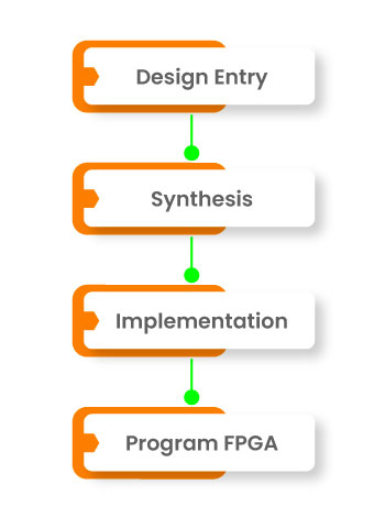
- Design Entry: Design entry can be done using two ways. One is through schematic; another is through Hardware Description Language (HDL). Tools with convert these schematic to HDL or HDL to schematic. Generally, for a design that deals more with complex systems, it is better to opt for HDL, a quicker, language-based process that rids you of the need to design in lower level hardware, while schematics is a good choice for someone who wishes to design hardware because it gives more visibility to the entire system. Schematic based approach tends to work better for low level or smaller designs whereas for complex designs better to go with HDL based approach.
- Synthesis: As the design entered by us is in form of code, it needs to be converted into a actual circuit what we intend to implement. This is done by the synthesis tools such as vivado etc. It converts the behavior code into gate level netlist where the entire circuit will be represented in form of gates, flip-flops and multipliers. The interconnections between them are also shown in a netlist. The process begins with a syntax check once you feed in your HDL based design. It is then optimized by the reduction of logic, elimination of redundant logic, and the reduction of the size of the design while simultaneously making it faster to implement. The last step is to map out the technology by connecting the design to the logic, estimating the associated time, and churning out the design netlists which are subsequently saved.
- Implementation: This phase is where the layout of your design will be determined and consists of three steps: translate, map, and place & route. The tools used in this step are provided by the FPGA vendors because they know best how to translate a synthesized netlist into an FPGA. The first step for the tools is to gather all the constraints that are set by the user together with the netlist files. These constraints can be regarding the assignment and position of the pins, the requirements regarding timing such as the maximum delay or the input period of the clock. Then the tool maps out the implementation by comparing the resource requirement specified in the files to the resources actually available on the FPGA being used. The circuit is divided into the logic blocks or elements in the form of sub blocks. As a result, your entire design is placed in specific logic blocks and is ‘mapped out’ into the FPGA. The next step is to connect and route all the signals accordance with the constraints set by the user between all the logic blocks and I/O blocks.
- Program FPGA: The last step in the process is to finally load the mapped out and completely routed design into the FPGA. For that reason, you will need to generate a Bit-Stream file and this bit stream file will be dumped onto your FPGA board using Flash programmer device. When you run your FPGA the board mimics your design functionality. This is the entire process for FPGA based design.Also in FPGA there is simulation checks which are done at each level. Behavior simulation is done at design entry level, Functional simulation is done post synthesis and Timing simulation is done at Implementation level.
ASIC Flow:
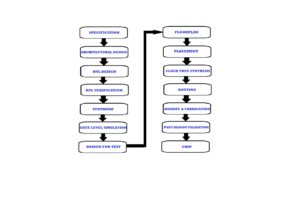
- Specification: The specification for the product is collected from the market or customer requirements. The specification also consists of what all features the product should consist of etc. These are generally collected by marketing people.
- Architectural Design: The architectural design consists of what all blocks the design should consist of and how they are connected in the design. They come up with a block diagram which includes all the above based on the specification. This architecture team will estimate the block area, how much power is required and cost for the design
- RTL Design: The RTL design is developed using HDL. It is developed based on the architecture design. It is written in Verilog or VHDL. This code describes how the data is transferred between different components in the design.
- RTL Verification: Verifying the developed design is done in this stage. Test cases will be developed to check the functionality of the design and if found any bug in the design, it is intimated to designer to modify it and release the new RTL. Verification itself takes 60 percent of total lifecycle time of chip development. This stage is very important as the design is tested for its functionality. Any bugs found post routing is difficult to correct and also post fabrication we cannot correct the design. So this is very important part of a chip development cycle.
- Synthesis: It is a process of converting the RTL code into gate level netlist. Up to RTL verification the design is technology independent. In synthesis process the design is converted into technology dependent. It is 3 stage process.
- Translation: RTL code is converted to Boolean expressions.
- Optimization: Boolean expression is optimized by SOP and POS optimization methods
- Mapping: In this the Boolean expression is converted into gates based on the technology and generates a gate level netlist. The inputs for synthesis are RTL code, .SDC and .LIB files. After the synthesis the generated outputs are gate level netlist and .SDC files.
- Gate Level Simulations: Gate level simulation is used to boost the confidence regarding implementation of a design and can help verify dynamic circuit behavior, which cannot be verified accurately by static methods. It is run after RTL code is simulated and synthesized into a gate-level netlist. Gate level simulation overcomes the limitations of static-timing analysis and is increasing being used due to low power issues, complex timing checks at 40nm and below, design for test (DFT) insertion at gate level and low power considerations. For DFT, scan chains are inserted after the gate-level netlist is created; gate level simulation is often used to determine whether scan chains are correct.
- Design for Testability: Design for testability (DFT) is a technique which facilitates a design to become testable after production. In this stage we put extra logic along with the design logic during implementation process which helps post production process. The DFT will make the testing easy at post production process. At this stage an ATPG (automatic test pattern generator) file will generate.
- Floorplan: The floorplan is the process of determining the macro placement, power grid generation and I/O placement. It is the process of placing blocks/macros in the chip/core area there by determining routing areas between them. It determines the size of the die and creates wire tracks for placement of standard cells. It creates power straps and specifies pg connection. It also determines the I/O, pin/pad placement information.
- Placement: Placement is the process of automatically assigning correct position to standard cells on the chip with no overlapping. By global placement outside of standard cells will be placed inside roughly. By the detailed placement the standard cells will place in site rows (legalize placement).In placement stage we check the congestion value by GRC map.
- Clock Tree Synthesis (CTS): In this stage we built the clock tree by using inverters and buffers. In the chip clock signal is essential to the flip flops, to give the clock signal from clock source we built the clock tree. It is the process of balancing the clock skew and minimizing insertion delay in order to meet timing and power.
- Routing: Before the routing stage the connection between the macros, standard cells, clock, i/o port are logical connections. In this stage we connect all the cells physically with the metal straps. Routing is divided as two parts 1) Global routing 2) Detailed routing. The global routing will tell for which signal which metal layer is used. Before the detailed routing all are the logical connections. In detailed routing the physical connections are done.
- Signoff & Fabrication: After the routing the physical layout of chip is completed. In signoff stage all the tests are done to check the quality and performance of the layout before tapeout. After this the design is converted into GDS II file. By the GDS II file information we fabricate the chip. The total design is converted into chip by the manufacturing process.
- Post Silicon Validation: Post-silicon validation is used to detect and fix bugs in integrated circuits and systems after manufacture. Post-silicon validation involves operating one or more manufactured chips in actual application environments to validate correct behaviors over specified operating conditions. The objective is to ensure that no bugs escape to the field. If there is any fault in the design then we modifies the design by repeating the steps. If there are no faults then chip will go to packaging.
- Chip: Finally we get the required chip which will be manufactured in bulk. If we use this process to produce only 1 chip, it costs a lot more than the actual chip cost after production. If we produce the chips in bulk, we can save the silicon wafer for producing more chips with single wafer and the cost of the production for each chip will be less than the cost for which it has been sold.
Comments are closed.
