Post CTS Optimization
Author : Adhila A., Physical Design Engineer, SignOff Semiconductors,
Author : Nisha K. P., Physical Design Engineer, SignOff Semiconductors
During Clock tree synthesis, buffers or inverters are added in the clock nets to achieve minimum Insertion delay and Skew, while meeting the clock DRV’s. Various optimizations are performed during CTS such as CCDO (Concurrent Clock and Data Optimization) and CTO (Clock Tree Optimization) . Once the CTS optimizations are done, the clock tree is fixed and routed. Further optimizations cannot be done on the clock tree except buffer sizing or gate sizing. Hence, post CTS, only data path can be optimized. The various post-CTS optimizations include : meeting DRV’s, Setup & Hold, Area & Power optimization, Congestion reduction.
DRV’s : Design Rule Violations
- Max Tran
- Max Cap
- Max Fanout
Causes :
- HVT cells give slower transition : The HVT cells have larger threshold voltages compared to LVTs and RVTs. Hence, they take more time to turn ON resulting in larger transition time.
- Weak Driver : The driver won’t be able to drive the load resulting in bad transition of the driven cell. Thus the delay increases.
- Load is more : The driving cell cannot drive load more that what it is characterized for. This is set in .lib using max cap value. If the load that a cell sees increases beyond its maximum capacitance value, then it causes bad transition and hence increases delay.
- Net length is large : Larger the net length, larger the resistance, worser the transition.Thus results in trans violation. The RC Value of a long net will increase the load seen by a cell causing max cap violations as well.
- Fanout is too large : If the fanout number increases beyond the limit of what the driver cell in characterized for, it causes max fanout violations. The increased load results in max cap violation which indirectly causes max tran violation as well.
Fixes :
1.Max Tran :
- Replace HVT cells with LVT cells.
- Upsize the driver.
- Reduce the net length by adding buffers. Longer the nets, larger the resistance. Putting a buffer at the middle of a long net splits the resistance into half.
- Reduce the load by reducing fanout and downsizing the driven cell.
2.Max Cap :
- Upsize the driver.
- Split long nets by buffering.
- Reduce the load by reducing the fanout (by load splitting) or by downsizing the driven cell.
3.Max Fanout :
- Reduce the fanout by load splitting by buffering or cloning.
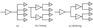
- Fig. (a) shows a buffer driving four other cells. In fig. (b), the load is split using Cloning. The first buffer is cloned and each buffer now drives half of the load. In fig.(c), the load is split using buffering. Two new buffers are added at the output of buffer A. Now buffer A is driving C1 and C2 and each of them are driving half of the load.
SETUP :
Reasons for Setup Violations:
- Tcomb :
- Tcomb delay is high.
- High RC metal might be used in Tcomb for routing which increases the net delay.
- More HVT Cells in data path.Lower drive strength cells in data path.
- Tsetup of capture flop is more.
- More negative skew : Launch clock is late and capture clock is early.
- Crosstalk delay :Signals switching in opposite direction resulting in more delay.
Fixes :
- Vt swapping : Replace HVT cells with LVT/ULVT cells.
- Upsize drivers in data path.
- For long nets, if adding a buffer can reduce RC, improve transition and hence improve timing, then add buffers.
- Reduce fanout.
- Layer optimization in data path : Use higher metals with lower RC Values to route in data path. This is preferred only if the timing path is critical.
- Fix cross talk using NDR Rules during routing stage.
HOLD :
Reasons for Hold Violations:
- Tcomb delay is less due to :
- Move LVTs and ULVTs in data path.
- High drive strength drivers in datapath.
- Told of capture is more.
- More positive skew.
- Cross Talk : Signals switching in same direction makes the data arrive early.
Fixes :
- Vt swapping : Replace LVT/ULVT cells with HVT cells.
- Add buffers in data path to increase data path delay.
- Downsize drivers in data path.
- Layer optimization in data path : Use lower metals with higher RC Values to route in data path.
- Fix cross talk using NDR Rules during routing stage.
AREA AND POWER OPTIMIZATION:
Need for area and power optimization:
- Clk cells are larger than normal cells. Hence, they take more area and consume more power.
- LVTs are used in clock path as they have less on chip variations and less short circuit power. But they have more subthreshold leakage power.
- Clock is a high switching net. Hence , it has more switching power.
Fixes :
- Area Optimization :
- Downsize Clock buffers if a smaller sized clock buffer can drive the same load.
- Power Optimization :
- Downsize Clock buffers if a smaller sized clock buffer can drive the same load.
- Replace HVTs with LVTs/ULVTs in datapath.
CONGESTION :
Causes :
The addition of extra buffers during CTS to achieve minimum skew and minimum insertion delay can cause congestion.
Fixes :
- Post CTS, we can’t move any clock cells. So, for a well optimized design Post CTS, we have to do a proper congestion driven placement keeping in mind the ulitization post CTS in the initial stages itself.
- Cell padding : In congestion prone area, cell padding should be applied for standard cells.
Comments are closed.
