What are GAA (Gate All Around) FET?
GAA is somehow similar to FinFETs except the conducting channel is surrounded by gate all around. Thus we get better gate controllability over the channel. The channel shape can be square or any other polygon shape.
Gate All Around Nanowire Field Effect Transistor:
Nanowire structure can be defined as an object with 1D aspect in which the length to width ratio is greater than 10nm and width is less than 10nm. The channel can be cylindrical in form and gate is circular (360 degree) in nature. The diameter of channel can be kept below 10nm without affecting it’s electrical properties.
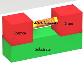
Figure 1: GAA Nanowire MOSFET
Need of GAA?
As we are moving towards nano-scale technology, the transistor density is increasing. So downscaling of transistors is required, but reducing the transistor size leads to degradation in device performance. This degradation is due to the short channel effects such as subthreshold current, drain induced barrior lowering etc. Several structures such as double gate, trigate transistors have replaced MOSFETs. Gate all around structures have shown the advantage of strong control over channel by gate in contrast to multi-gate FETs. It has the highest conductivity and electrical properties.
Structure :
Basically in GAA MOSFETs, the gate is wrapped all around the channel. By all-around covering of the gate over a channel, it is a promising structure of better gate control and better short channel performance. There are undoped and doped channels, both the type of channels are used in GAA technology. The drain and source terminals are formed at the outer sides of the channel. Similar to MOSFET.
GAA also has two types:
- n-channel GAA in which channel is doped with n+ type impurity.
- p-channel GAA in which channel is doped with p+ type impurity.
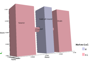
Figure 2: Pentagonal GAA Nanowire MOSFET(channel is surrounded by gate)
Gate Length :
Normally the gate length is defined by the length of gate materials which is wrapped around the channel whereas in Nanowire technology, the gate length is slightly larger than channel length which is called as gate overlapped thickness. Gate length also defines the controllability of the gate over the channel and effective electric field of the channel. The shortchannel effects like subthreshold slope and drain induced barrier lowering(DIBL) are anti-proportional to gate length such as they are increasing with reduction in gate length. Other parameter like threshold voltage Vt is directly proportional to gate length such as It is decreases with reduction in gate length.
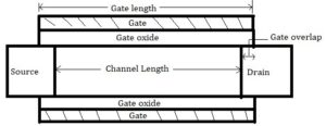
Figure 3: Cross section of Nanowire FET
Doping Concentration :
Basically doping is a process of adding impurity in a particular region. Doping is done to enhance the conductivity, to achieve excellent electrostatic field, higher mobility and to improve drain current of the device. In NWTs.
Channel doping : channel is doped with n+ in n-type Si-NWTs or p+ in p-type Si-NWTs impurity. It would be vary with the channel length.
Substrate doping :
Source/Drain doping : highly doped; n-type Si-NWTs has p+ doping and p-type Si-NWTs has n+ doping.
Channel Diameter :
Channel Diameter affects the drain current and mobility of devices. Cross section area depends on diameter and shape of the channel, which defines the mean free path of electrons and conductivity of the channel. Higher cross section area derives the higher drive current and higher switching. By using of Nanowire FET, the diameter of channel can be used in the ranges of 5nm without degrading the characteristics of devices.
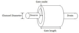
Figure 4: Nanowire showing different parameters
Advantages :
- Better gate controllability as gate is all around the channel.
- Leakage current is almost negligible (leakage current also based on the shape of channel).
- Effect of Short channel is very less.
- High drain current.
- Low Subthreshold slope.
- Corner effect is very less (negligible if channel shape is cylindrical).
Disadvantages :
- Difficulty in fabrication as the gate is all around the channel so more chances of forming a ruptured channel during fabrication.
- Heating Problem.
Comments are closed.
