Routing optimization and Chip Finishing
Author: Avik Sumed Arun, Physical Design Engineer, SignOff Semiconductors Pvt Ltd
ROUTING OPTIMIZATION
- Routing optimization is a step performed after detailed routing in the flow.
- Inaccurate modeling of the routing topology may cause timing, signal integrity and logical design constraint related violations.
- This may cause conditions wherein fixing a violation would create other violations and many such scenarios may cascade to make it very difficult for timing closure with no timing DRCs.
- Hence it is necessary to fix and optimize the routing topology.
- Routing optimization involves-
- Fixing timing violations.
- Fixing LVS (opens & shorts).
- Fixing DRCs.
- Fixing Timing DRCs (Meet max transition, max capacitance and max fanout).
- Finding & Fixing Antenna violations (using jumpers and antenna diodes).
- Area and Leakage power recovery.
- Fixing SI related issues.
- Redundant via insertion.
This post will concentrate on Finding & Fixing Antenna violations and Redundant via insertion. The other topic will be covered in subsequent posts.
Antenna Violations
- During IC fabrication, the wafer usually undergoes various processing steps, such as metalization (laying of metal wires) and etching (to make the surface flat). During the metalization step, few of the nets connecting the gate terminals can be floating as upper metal layers have not been fabricated yet. In the plasma etching process (widely used in recent fabrication processes), there may be accumulation of unwanted electrostatic charges on these floating nets, which act as antennas.
- Typically, in ICs nets are driven either from source or drain of the device and connects a receiver gate terminal over a gate oxide. Gate oxides being thin for higher technology nodes, are susceptible to electrostatic discharges and are in danger of getting ruptured due to higher potentials than the breakdown voltage.
- When these charges flow through the devices it can rupture the gate of the device, there by leading to a total chip failure. This phenomenon of an electrostatic charge being discharged into the device is known as “antenna effect”.
- Every FAB have their own set of rules (depends on the type of technology the ICs are being fabricated) to avoid antenna violations during IC design.
In order to prevent antenna problems, tools verify that for each input pin the metal antenna area divided by the gate area is less than the maximum antenna ratio given by the foundry:
(Antenna area) ⁄ (Gate area) < (Max Antenna ratio)
Gate area: The are of transistors which is the intersection of the diffusion and the polysilicon layers.
Antenna area: Total area of metal connected to gate terminal.
Max Antenna Ratio: Maximum allowable ratio of Antenna area to Gate area.
Fixing antenna violations
There are many techniques to fix antenna violations. The widely used techniques are described in this post.
Antenna Diode:
- Reverse biased diodes (Zener diodes) inserted close to the gate terminal to provide a discharge path for the electrostatic charges during plasma etching.
- This reverse biased diode will not affect the operation of the circuit as it will conduct only if the potential reaches its breakdown potential, thus protecting the respective gate from damage.
- The general rule of practice is to use an n-type diode as p-type diodes requires extra n-well biasing.
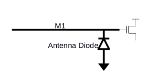
Fig1: Antenna Diode.
Limitations of using antenna diodes:
- Wastage of core area – If the number antenna violations is large, the overuse of antenna diodes eats up the core area meant for standard cells.
- These diodes eat up extra placement and routing silicon resources which becomes a costly during fabrication.
- Potential Forward biasing of diode – The antenna diodes are usually placed in a back to back fashion where there is an antenna violation. If they are not biased (reverse biased) in a correct way, there is a potential of one of the diodes to get forward biased. This is usually seen in low power designs when one of the power source gets switched off. One such case is shown in the example figure below. Here D2 is always in a reverse biased condition. But in the case of D1, if the cathode is turned off, it gets forward biased due to the reverse biasing of D2. Hence, a lot of care must be takes such that both anode and cathode are in the same potential or the anode must be at ground potential.
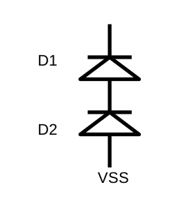
Fig2: Back to Back connected Antenna diode.
- Leakage Power – Antenna diodes contribute to the total leakage power which may affect the working of the design. Hence overuse of these diodes must be avoided.
Use of Jumpers (metal Hopping):
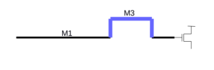
Fig3: Jumpers (metal hopping)
- One of the most widely used ways to fix antenna violations during routing optimization.
- By definition, antenna violations occur in cases where the nets connected to gate terminals are long, which can lead to a large amount of static charge accumulation leading to damage of gate oxide.
- This can be fixed by using jumpers which is basically jumping to higher metal layers to keep the total length of the lower metal layer directly connecting the gate terminals below the maximum length and also floating as the charges don’t flow into the gate terminal.
- During fabrication only nets that are in the lower metal layer are fabricated first, thus leaving a gap (floating) where the jumping to higher metal layers occurs. This reduces the area for static charge accumulation and hence keeps the gate relatively safe until the upper metal layer is stacked and connected to the other part of the lower metal layer.
- Using jumpers nearer to the gate terminal makes the device relatively safer from antenna effect.
- It is to be noted that jumping from a higher metal layer to lower metal layer cannot be done as lower layers are already fabricated and this causes the flow of static charges leading to the damage of devices connected.
- In the case of antenna violations on analog blocks, jumpers are to be added very close to the analog pins.
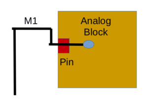
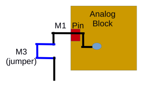
Fig4: Jumper insertion for analog block.
- For high fanout nets such as reset and scan enable, with large number of sinks, the location of jumpers must be selected such that fixing violation at a point adjacent to a group of sinks via jumpers fixes multiple violations on the group, instead of individually fixing them.
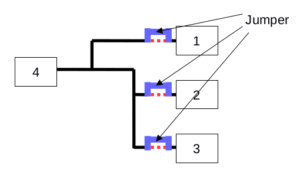
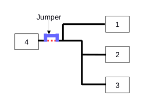
Fig5: Jumper insertion for High Fanout nets.
- To make use of jumpers at the point of violation make sure that there are no routing blockages for the higher metal layer in that region.
- It is to be noted that using metal jumpers are the most widely used method to fix antenna violations during post-route optimization and antenna diodes are used as last resort where jumpers cannot be added in regions where routing blockages are present or adding them may cause other violations such as SI related or congestion at higher layers.
Redundant Via Insertion / Double Via Insertion.
- During IC fabrication, there may be partial or complete via failure due to various reasons such as cut misalignment, electro migration and thermal stress induced voiding.
- A partial via failure increases the resistance of the signal nets and may increase the delay causing difficulty in timing closure. Whereas a complete via failure will result in broken nets.
- This leads to increase in yield loss and hence is critical to fix this issue.
- To fix yield loss due to via failure, a good practice is the insertion of redundant vias adjacent to single vias for support.
- Redundant vias are basically extra single vias on minimal width nets.
- It is to be noted that redundant vias are required for support to increase the yield, unlike muli-cut vias on wide nets for functionality purposes.
- Although redundant via insertion is a step in Design for Manufacturability (DFM) it is more advantageous to insert redundant vias in the post-route optimization stage or during the detailed routing stage. This is because during the DFM stage the layout is almost complete and can be modified only slightly without causing other cascaded violations. Hence this restricts the insertion of redundant vias at single via points, resulting in an increasing chance of yield loss due to via failure.
- If the amount of redundant vias inserted are not guided, the yield and reliability of the design may be adversely affected due to pattern distortion of these vias may become as serious problem.
- The advantages of redundant vias are-
- Nets are less likely to break.
- Yield is improved.
- Decrease in the resistance of the vias.
- Avoids increase of net delay due to partial via failure.
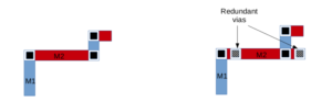
Fig6: Redundant via insertion.
Chip Finishing
Chip finish is a stage after post-route optimization, where filler cells and metal fills are added to meet the DRC rules. The different steps in chip finish are briefly described below.
Inserting Filler Cells
- Filler cells are used for rail continuity and to fill up gaps between standard cells in the rows, thereby reducing the DRC violations created by the base layers.
- Filler cells are physical-only cells designed in such a way that they contain only n-well, p-well & power rails.
- Although the standard cells have implant layers in them, meeting the width and spacing DRC rules may not be feasible without abutting filler cells with respective implant layers.
- It is also possible to reduce the IR drop by inserting de-cap filler cells, but this comes at a cost of higher leakage currents.
Inserting Metal Fills (Dummy Metal Fills)
- The metal fills (also called dummy metal fills) are small, floating metal nets, inserted after post-route optimization in order to maintain uniformity in metal layer density, in empty spaces in the design.
- These are added to meet the metal density DRC rules which are mandatory by most manufacturing processes.
- The process of adding metal fills is as follows-
- To maintain uniformity for any metal layer, we have window based density rules.
- For each window metal density will be specified.
- If the utilization of metal in a window is less than that given in DRC rule deck, then we add dummy metals to overcome density DRC.
- The prerequisites for adding metal fills are as follows-
Comments are closed.