STA – Part1
Author : Nishant Lamani, Physical Design Engineer, SignOff Semiconductors,
Author : Abhishek Kumar, Physical Design Engineer, SignOff Semiconductors
What is STA ?
- Static timing analysis is one of the techniques used to verify the timing of a digital design.
- STA is static since the analysis of the design is carried out statically and does not depend upon the data values being applied at the input pins of the design.
- STA is a complete and exhaustive verification of all the timing checks of a design.
Why we do STA ?
- Timing analysis methods such as simulation can only verify the portions of the design that get exercised by simulus.
- Verification through timing simulation is only as exhaustive as the test vectors used.
- To simulate and verify all the timing conditions of a design with 10-100 million gates is very slow and timing cannot be verified completely.
- So, STA on the other hand provides faster and simpler way of checking and analyzing all the timing paths in the design for any timing violations.
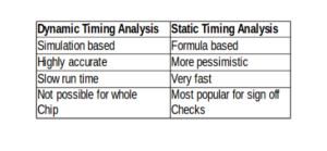
Dynamic Timing Analysis (DTA) :
- Dynamic Timing Analysis requires a comprehensive set of input vectors to check the timing paths in the design.
- It determines the full behaviour of the circuit for a given set of input vectors.
- Dynamic simulation can verify the functionality of the design as well as timing requirements.
Example : If we have 100 inputs, then we need 2 to the power 100 simulation for complete the analysis. The amount of analysis is astronomical compared to static analysis.
Difference between DTA and STA ?
Input and Output Files of STA :
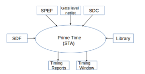
Figure 1 : Input & Output file for STA
Basics of Setup and Hold Time :
To understand why setup and hold time requirement arises in a flip-flop, we have to look at the building blocks of a flip-flop which includes inverters and transmission gates. A transmission gate is a parallel connection of NMOS and PMOS with complementary control inputs to both. Whenever both NMOS and PMOS are turned on, any signal 1 or 0 passes equally well without degradation. Two back-to-back inverters form a latching circuit as it retains a logic value.
Figure 2(i) : Positive Edge Triggered D Flip-Flop circuit
D flip-flop : Normal operation
Initially when D=0 and CLK is low, then TG1 & TG4 turn on and TG2 & TG3 are turned off. The input follows the path D-P1-P2-P3 and finally data at P3 is 0.
Figure 2(ii) : Operation of D Flip-Flop when CLK = 0
When CLK is high, then TG2 & TG3 turn on and TG1 & TG4 are turned off. The data 0 comes out of TG2 and follows the path TG2-P1-P2-TG3-P4-P5-Q . Finally we get Q = 0. The output arrives at positive edge of CLK so it is a positive edge triggered flip-flop.
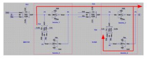
Figure 2(iii) : Operation of D Flip-Flop when CLK = 1
When CLK is low there is no change in output. Any change in input appears at P3 but it is reflected at the output only when CLK turns high again.
Setup Time :It is the minimum amount of time before the active edge of clock for which the data must be stable for it to be latched correctly.
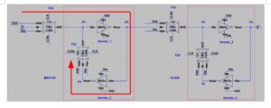
Figure 2(iv) : Setup requirement of a flip-flop
Setup requirement of a flip-flop :When D = 0 and CLK is low, input follows the path D-P1-P2-P3 and reches the input of TG2. The time taken by data D to reach the input of TG2 is called the setup time of a flop. If data changes in this time it will not be able to reach input of TG2 and when TG2 turns on, there might be two different data reaching node P1, which will cause meta-stability.
Hold Time :It is the minimum amount of time after the active edge of clock during which data must be stable for data to be latched correctly.
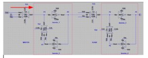
Figure 2(v) : Hold requirement of a flip-flop
Hold requirement of a flip-flop :It arises because of the finite delay in ramping up of the CLK and CLKb signals which controls the switching of transmission gates. TG takes some time to switch on or off, known as hold time of a flop. So it is necessary to maintain a stable value at D pin to ensure a stable value at node P1 which is translated to output.
Basic Terminology in STA :
Setup Time :The minimum time before the active edge of the clock, the input data must remain stable is called the setup time.
Hold Time : The minimum time after the active edge of the clock, the input data must remain stable is called the hold time.
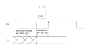
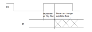
Figure 3 : Setup & Hold time
Launch and Capture edge :
- Launch edge is that edge of the clock at which data is launched by a flip flop.
- Capture edge is that edge of the clock at which data is capture by a flip flop.
Launch and Capture flip flop :
- The flip-flop that launches the data is a launch flip flop.
- The flip-flop that captures the data whose setup/hold time must be satisfied is a capture flip flop.
Setup and Hold timing checks between launch and capture flip flop :
Setup timing checks :
- The setup check ensures that the data is available at the input of the flip-flop before the active edge of the clock.
- The data should be stable for a certain amount of time, namely the setup time of the flip-flop, before the active edge of the clock arrives at the flip-flops, so that the data is captured reliably into the flip-flop.
- The setup check ensures that the data launched from the previous clock cycle is ready to be captured after one cycle.
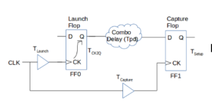
Figure 4(i) : Setup check between two flops
- Setup equation,
[Tlaunch + TCK2Q + Tpd] < [Tcapture + TCLK – TSetup]
Hold timing checks :
- The hold check ensures that the data is available at the input of the flip-flop after the active edge of the clock.
- The data should be stable for a certain amount of time, namely the hold time of the flip-flop, after the active edge of the clock arrives at the flip-flops, so that the data is captured reliably into the flip-flop.
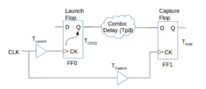
Figure 4(ii) : Hold check between two flops
- Hold equation,
[Tlaunch + TCK2Q + Tpd] > [Tcapture + Thold]
Slack :
Slack is the difference between the required time and the time a signal arrives.
- Data Arrival Time :This is the time required for data to travel through data path.
- Data Required Time :This is the time taken for the clock to traverse through clock path.
Setup Slack = Data Required Time – Data Arrival Time
Hold Slack = Data Arrival Time – Data Required Time
Slew :
Slew is the transition time of a signal, the time it takes for a signal to change between two specific levels.
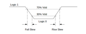
Figure 5 : Slew / Transition Time
Propagation delay :Propagation delay is the time required for the input to be propagated to the output. In other words, the propagation delay of a logic gate is defined as the time it takes for the effect of change in input to be visible at the output.
Skew : Skew is the difference in the arrival of the clock at two consecutive clock pins of sequential elements.
- Positive Skew :If the capture clock comes late than launch clock then it is called positive skew.
- Negative Skew :If the capture clock comes early than launch clock then it is called negative skew.
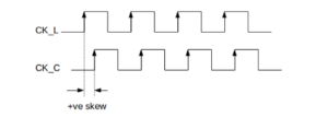
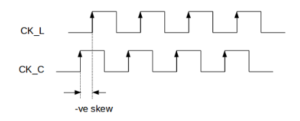
Figure 6 : Positive & Negative Skew
Global Skew :It is defined as the difference between the maximum insertion delay and the minimum insertion delay between two flip flops.
Useful Skew :If the clock is skewed intentionally to resolve the violations, it is called as useful skew.
Clock Latency :Clock latency is the time it takes from clock source to end point.
- Source Latency : Source latency, also called as insertion delay, is the delay from clock source to the clock definition point.
- Network Latency : Network latency is the delay from clock definition point to clock pin of the register (sink point).
Clock Latency = [ ( Source Latency ) + ( Network Latency ) ]
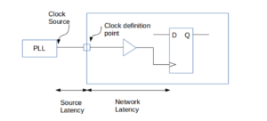
Figure 7 : Source & Network Latency
Clock Uncertainty :Clock uncertainty is the deviation of the actual arrival time of the clock edge with respect to ideal arrival time. The deviation happens mainly due to jitter and noise.
- PrimeTime subtracts setup uncertainty value from the data required time when it checks setup time (maximum paths).
- PrimeTime adds hold uncertainty value to the data required time when it checks the hold time (minimum paths).
Jitter : Clock jitter refers to the temporal variation of the clock period at a given point — that is, the clock period can reduce or expand on a cycle-by-cycle basis.
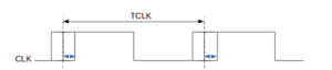
Figure 8 : Jitter
Common sources of Jitter are,
- Internal circuitry of the phase-locked loop (PLL)
- Noise from a crystal
- Interconnect variations
- Temperature
- Power supply
False Path : A false path is a path existing in a design which should not be analysed for timing. For example,
- A path between two multiplexed blocks that are never enabled at the same time. In below diagram timing path starting from CLK pin of FF1 and ending at D pin of FF3 is a false path because it can’t exist in circuit operation because of inverted select signals at the multiplexer select pins.
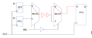
Figure 9(i) : Falsepath between two MUX
- A path between flip-flops belonging to two clock domains that are asynchronous with respect to each other.
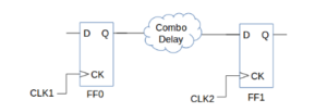
Figure 9(ii) : Falsepath between two flops
Declaring a path to be false removes all timing constraints from the path and the advantage is that the analysis time and effort are reduced, thereby allowing the STA tool to focus only on the real paths.
Multicycle Path :A path that is designed to take more than one clock cycle for the data from launch flop to propagate to the capture flop. The combinational data path between two flip-flops can take more than one clock cycle to propagate the data. In such cases, the combinational path is declared as a multicycle path. For example,
The path from FF4 to FF5 is designed to take two clock cycles rather than one. However, by default, PrimeTime assumes single-cycle timing for all paths. Therefore, we need to specify a timing exception for this path.
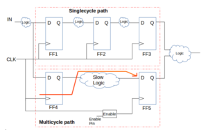
Figure 10 : Single & Multicycle Path
Halfcycle Path : A path which requires only half cycle to capture the data. It is formed when data is launched on positive edge of the clock and captured on negative edge of the clock or when data gets launched on negative edge of the clock and gets captured on positive edge of the clock.
In such paths, setup check become more tight as setup gets only half cycle while hold constraint is relaxed by half cycle.
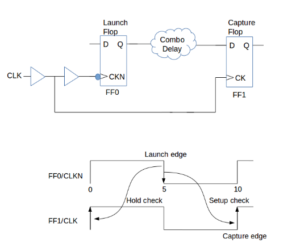
Figure 11: Half-cycle Path
The falling edge occurs at 5ns and the rising edge occurs at 10ns. Thus, the data gets only a
half-cycle, which is 5ns, to propagate to the capture flip-flop. While the data path gets only half-cycle for setup check, an extra half-cycle is available for the hold timing check.
The hold check always occurs one cycle prior to the capture edge. Since the capture edge occurs at 10ns, the previous capture edge is at 0ns, and hence the hold gets checked at 0ns. This effectively adds a half-cycle margin for hold checking and thus results in a large positive slack on hold.
Cross-talk Noise :It is undesired change in the output values of victim due to switching in the input of aggressor. If one net is switching and other is at a constant value , the switching net may cause voltage spikes on other net. This is called as cross talk noise. Cross talk noise is evolving as a key source in degrading performance and reliability of high speed integrated circuits.
Cross-talk Delay :When there is some delay in output transition of victim due to input transition of aggressor, it is called as cross talk delay. It occurs when some transition is happening in both the nets. Cross talk delay depends on the switching direction of the aggressor and victim nets too. If input transitions occur in same direction then output transition of victim becomes faster and if input transitions occur in opposite directions then output transition of victim becomes slower and delay is more which may violate setup time.
Read our blog on wire modelling and cross-talk for more information.
Virtual Clock :
- A virtual clock is a clock that exists but is not associated with any pin or port of the design.
- It is used as a reference in STA analysis to specify input and output delays relative to clock.
- A virtual clock can be defined with no specification of the source port or pin.
- Virtual clock are required to constraint the input port to register timing path and register to output port timing path.
- Advantage of virtual clock is we can specify the desired latency.
Minimum Pulse Width Violation :
- Minimum pulse width is an important check for clock, for the proper performance of the sequential circuit.
- Pulse width check ensure the width of the clock signal is above minimum value.
- When the width of the clock signal is below minimum value, we get minimum pulse width violation and signal shrinks.
- This is due to unequal rise and fall delay of the combinational cell.
- If the rise edge is more than the falling edge of a clock, then the output clock will have less width than the input clock.
- So, when this clock signal is passed through the series of buffers, the width of a signal keeps on decreasing and at a point when the buffer delay is more than the clock width, pulse get absorbed. This is know an pulse absorption.
- So it is better to have equal rise and fall edge in order to avoid to pulse width violation.
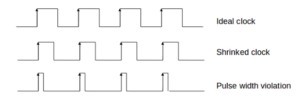
Figure : Pulse Width Violation
Read our blog on pulse width reduction to know how and why pulse width violation occurs.
What is the difference between clock buffer and normal buffer ?
- Clock buffer have equal rise time and fall time, therefore pulse width violation is avoided.
- Normal buffers may not have equal rise and fall time.
- To make equal rise and fall time in a clock buffer we make PMOS width nearly 2 – 2.5 times the width of NMOS. Hence it consumes more power.
- Clock buffers are usually designed such that an input signal with 50% duty cycle produces an output with 50% duty cycle.
Comments are closed.