LOGIC GATES
Authors : Poojitha Palem, Digital Design Engineer, SignOff Semiconductors
Sachidananda Reddy, Digital Design Engineer, SignOff Semiconductors
We hope you had a good understanding of Number Systems which is available @ Number Systems. For building hardware, we need logic gates, combinational circuits and sequential circuits which takes input in the form of binary numbers. The main building blocks to design combinational and sequential circuits are logic gates which is explained below.
TRUTH TABLE:
Truth Table describes how a logic circuit’s output depends on the logic levels present at the circuit’s inputs.
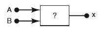
Note that the number of input combinations will be equal to 2n for an n-input truth table.
LOGIC GATES:
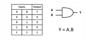
AND GATE:
The AND operation is performed same as the ordinary multiplication of 1s and 0s. The output of AND gate becomes 1 only when all the inputs are 1. Hence AND gate is also called an all or nothing gate.
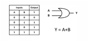
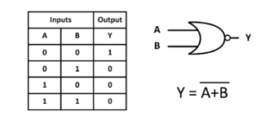
OR GATE:
The output of OR gate becomes 1 even if one of its inputs is 1. Hence OR gate is also called an any or all gate. It can also be called as inclusive OR gate because it includes the condition both the inputs can be present.
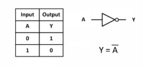
NOT GATE:
NOT gate is also called an Inverter. The output of NOT gate is always the complement of its input.
UNIVERSAL GATES:
The NAND and NOR gates are called as universal building blocks. These gates can perform all the three basic logic functions (AND, OR, NOT).
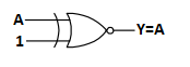
NAND GATE:
The NAND gate operates like an AND gate followed by an INVERTER.

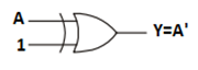
NAND gate as an inverter: A NAND gate can be used as an inverter by connecting all the input terminals together. It also acts as a controlled inverter as shown in the figure.
![]()
Bubbled NAND gate: It is equivalent to OR gate.
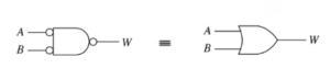
Bubbled OR gate: The OR gate with inverted inputs is called as Bubbled OR gate which is also called as negative OR gate. NAND gate is also called as an active low OR gate since its output becomes high even if any of the input is 0.
NOR GATE:
The NOR gate operates like an OR gate followed by an INVERTER.
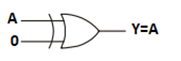
NOR gate as an inverter: A NOR gate can be used as an inverter by connecting all the input terminals together. It also acts as a controlled inverter as shown in the figure.
![]()
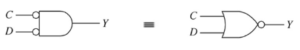
Bubbled NOR gate: It is equivalent to AND gate.
![]()
Bubbled AND gate: The AND gate with inverted inputs is called as Bubbled AND gate which is also called as negative AND gate. NOR gate is also called as an active low AND gate since its output becomes high only when all its inputs are equal to 0.
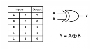
EXCLUSIVE-OR (X-OR) GATE:
For two input X-OR gate,the output becomes 1 only when the inputs are not equal. So, it is called as anti-coincidence gate or inequality detector. The output becomes 1 only when exclusively one of its input is 1 (it excludes the condition when both inputs are 1).

For three or more variable X-OR gate, the output becomes 1 only when odd number of inputs are 1. It is also called as odd function.
X-OR gate as an inverter: An X-OR gate can be used as an inverter by connecting one of its input to 1.
X-OR gate as a buffer: An X-OR gate can be used as a buffer by connecting one of its input to 0.
X-OR gate can also act as a controlled inverter, that is, one of its inputs can be used to decide whether the signal at the other input will be inverted or not.
If A^B=C then A^C=B, B^C=A and A^B^C=0
EXCLUSIVE-NOR (X-NOR) GATE:
X-NOR gate is a combination of X-OR gate and NOT gate.
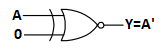
X-NOR gate as an inverter: An X-NOR gate can be used as an inverter by connecting one of its input to 0.
X-NOR gate as a buffer: An X-NOR gate can be used as a buffer by connecting one of its input to 1.
Note: For odd number of inputs, (A^B)^C = A^B^C
For even number of inputs, ((A~^B)~^C)~^D = A~^B~^C~^D
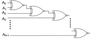
Question to try:
N number of XNOR gates are connected as shown below. How does this circuit work?
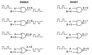
ENABLE AND INHIBIT(DISABLE) CIRCUITS:
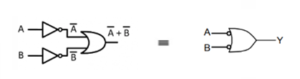
AND, OR, NAND and NOR gates can be used to control the passage of an input signal to the output. In the following figure, the logic level at the control input (B) determines whether the input signal (A) is enabled to reach the output or inhibited from reaching the output.
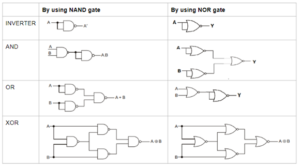
ALL BASIC GATES BY USING NAND AND NOR GATES:
IMPLEMENTATION OF MULTILEVEL DIGITAL CIRCUIT USING NAND GATES ONLY:
To obtain a multilevel NAND circuit from a given Boolean function, the procedure is as follows:
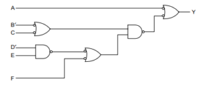
Consider a Boolean function Y = A + (B′ + C) (D′E + F)
Step-1: First draw the logic diagram using basic gates. (Her, it is assumed that both normal and complemented forms are available i.e., no need of inverter)
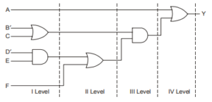
Step-2: Convert all AND gates to NAND using AND-invert symbol and all OR gates to NAND using Invert-OR symbol.
Step-3: From the above figure, it is very clear that only two inputs D′ and E are emerging in the original forms at the output. Rest i.e., A, B′, C and F are emerging as the complement of their original form. So we need an inverter after inputs A, B′, C and F or alternatively we can complement these variables as shown in figure.
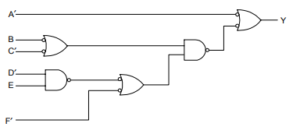
Step-4: Replace bubbled OR with NAND.

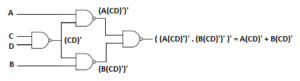
Questions to try:
Implement Y=(A+B)(C’+D’) by using minimum number of NAND gates? (Find the solution at the last page)
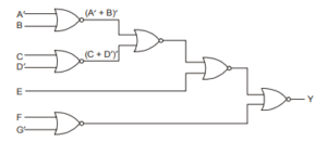
IMPLEMENTATION OF MULTILEVEL DIGITAL CIRCUIT USING NOR GATES ONLY:
To obtain a multilevel NAND circuit from a given Boolean function, the procedure is as follows:
Consider a Boolean function Y = [ (A’+B).(C+D’) ]E + (F+G’)
Step-1: First draw the logic diagram using basic gates. (Her, it is assumed that both normal and complemented forms are available i.e., no need of inverter)
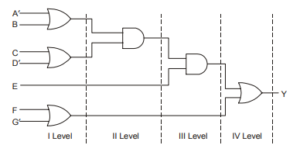
Step-2: Convert all OR gates to NOR using OR-invert symbol and all AND gates to NOR using Invert-AND symbol.
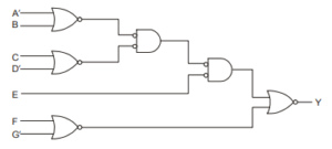
Step-3: From the above figure, it is clear that all the input variables are imerging in the same form at the ouput Y as they were at input. Therefore there is no need of inverter at inputs or complementing the input variables. So, replace bubbled AND gate with NOR gate.
Why NAND is more preferable when compared with NOR?
NAND offers less delay: NAND has lesser delay than NOR due to the NAND PMOS (size 2 in parallel) when compared to NOR PMOS (size 4 in series). The logical effort of NAND gate is less than that of NOR gate.
NAND occupies less area: When compared with NAND, NOR occupies more silicon area. The size will increase as the number of inputs are increased.
Questions to try:
Can you find any other universal gates other than NAND and NOR gates? If so, please post your answers in the comment section.
Solution:
(A+B)(C’+D’) = A(C’+D’) + B(C’+D’) = A(CD)’ + B(CD)’ = ( (A(CD)’ + B(CD)’)’ )’ = ( (A(CD)’)’ . (B(CD)’)’ )’
Comments are closed.
