What are FinFETs?
FinFETs are non-planar transistors built on SOI or Bulk substrate. FinFET describes any fin-based, multi-gate transistor architecture, regardless of the number of gates. The term “FinFET” (fin field-effect transistor) was coined by University of California, Berkeley, researchers (Profs. Chenming Hu , Tsu-Jae King-Liu and Jeffrey Bokor) in 2001 to describe a nonplanar, double-gate transistor built on an SOI substrate.
Principle:
In FinFETs, the channel is formed by a thin fin wrapped by a gate over a lightly doped thin substrate. The gate interfaces with the channel from three sides providing better electrostatic control of the with reduced leakage current and reduced short-channel effects.
The FinFET has a conducting channel wrapped by a thin silicon “fin”.
Why do we need FinFETs?
As the devices sizes shrunk, in lower technology nodes, like 22nm, with the scaling in channel length, area, power and operating voltage, the short channel effects started becoming more dominant, reducing the performance of the device. To overcome this issue, a new FET design named “FinFET” is developed.
Structure:
The FinFET structure consists of a thin fin of silicon on a substrate with the gate wrapped over the fin. The two sides of the fin which are not wrapped under the gate forms the source and the drain. The gate orientation is at right angles to the vertical fin. The channel is formed in the fin area wrapped under the gate.
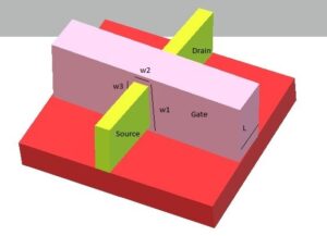
Figure 1: Structure of FinFET
The gate surrounds the channel from three sides providing better electrostatic control of the channel. Such a gate structure is known as a tri-gate structure and can fully deplete the channel of carriers, providing better electrical characteristics with reduced leakage current and reduced short-channel effects. This design is called the FinFET because its Si body resembles the back fin of a fish.
In planner CMOS devices, the channel is horizontal while in FinFETs, the channel is vertical. The width of the FinFET is dependent on the height of the Fin.
In Fig.1, w1 = w3 = Height of the Fin, w2 = Thickness of the fin.
The width of the channel is given in the equation given below :
Effective Channel Width = (2 * Height of Fin) + Thickness of the fin
W= (2*w1) + w2
Effective Channel Length = Length of the gate = L
This type of gate structure provides improved electrical control over the channel conduction and helps reduce leakage current levels and overcome some of the short-channel effects.
Operation of an n-Type FinFET:
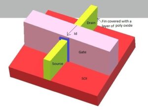
Figure 2 : Current flow through the channel
ON Condition: Vgate > Vth, Vdrain = ‘+’ ve, Vsource = 0V.
When the gate electrode is given a voltage higher than the threshold voltage, the region beneath the gate is inverted and forms a channel, providing a conducting path between the source and the drain. The current flows from Drain to Source in the channel as represented in Fig. 2. Both sides of the channel conduct, delivering more current than the planar CMOS transistor, as FinFETs have wider active current area and higher electron mobility.
Off Condition: Vgate < 0V, Vsource = 0V, Vdrain = ‘+’ve.
Transistor is in OFF condition and since the gate controls the channel from both sides, the leakage is reduced better than a planar CMOS transistor.
Advantages of FinFETs over CMOS:
- Superior gate control of the channel even at low voltages.
- Greatly reduced short channel effects. (Hence guard banding needed is reduced).
- High integration density due to 3D structure.
- Channel doping is less. Hence, less dopant induced variations and better performance.
- Works at lower operating voltage (Hence lower static and dynamic power)
- Better performance for a given power budget.
- FinFETs have lower DIBL. Hence reduced sub-threshold leakage.
- For memory designs, FinFETs have lower retention voltage for SRAMs compared to planar.
- The back-end design process is essentially the same for both FinFETs and CMOS. Hence a significant amount of the design flow associated with the back-end remains intact.
Disadvantages of FinFETs over CMOS:
- FinFETs are complex devices to model.
- FinFETs are 3D structures which needs high aspect ratio etching with non-uniform pitches or locally varying pitches, which is complex. Thus FinFETs have a significant numbers of restricted design rules (RDR).
- The body biasing techniques commonly used in planars is less effective in FinFETs due to the fully-depleted channel.
- Accurate FinFET parasitic extraction is more complicated.
Comments are closed.
