Getting started with Ubi, std cell design & layout #1
Author : Abhishek Kumar, Physical Design Engineer, SignOff Semiconductors
Author: Adhila A, Physical Design Engineer, Signoff Semiconductors
Why Ubuntu/Linux?
“Lot of freeware VLSI CAD tools work well on Ubuntu. Learning Linux, shell commands/scripts, awk, grep, sed, perl & shell will be very easy on Ubuntu, these are basic things any VLSI engineer has to know & this knowledge makes him faster”
Simple method to set up Ubuntu on your Windows machine.
1. Step 1
Download Wubi installer. Link – https://github.com/hakunam/wubiuefi/releases/download/16041r311/wubi16041r311.exe
2. Step 2
Download the Ubuntu Image. Link http:/releases.ubuntu.com/16.04/ubuntu-16.04.3-desktop-i386.iso
3. Step 3
Create a directory in any drive which have more memory, name it as Ubuntu. Copy downloaded Wubi Installer & Ubuntu image in that directory (same directory).

4. Step 4
Double click on Wubi Installer. Following window will be popped up on clicking Wubi,
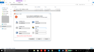
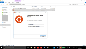
Assign Installation size, username & password (Use simple password, which you will not forget). Wubi will be launched in few seconds & it will ask for Reboot. On Rebooting, Ubuntu installation starts. Follow the instruction to complete the installation.
Installing LTSpice & Electric on Ubuntu
Use this link: http:/cmosedu.com/jbaker/students/wenlan/Electricwu.htm
Feel free to contact us through comment section, in-case of any queries
Getting started with LTSpice
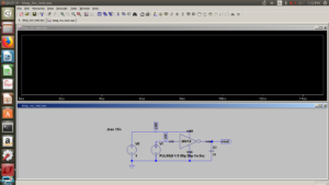
Ltspice is a freeware tool provided by Linear Technology to design and simulate SPICE models of various electronic circuits. Let us model and simulate a CMOS Inverter using Ltspice IV and perform Transient analysis.
Creating schematic of CMOS Inverter :
1.Open LTspice. Start by creating a new schematic. Go to File –>New Schematic. Else you can click on New Schematic icon as shown.
![]()
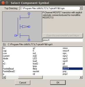
2.Select components from library by clicking on component icon.
![]()
3.Select pmos4 and then nmos4. Now specify the parameters of pmos and nmos by right clicking them respectively. Change the model name as per the Tech file.
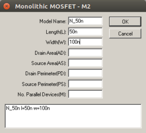
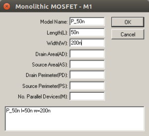
4. Attach the Tech file to the schematic using T key. Select spice directive and specify the path of Tech file. A sample 50nm technology file can be downloaded from following link, http:/cmosedu.com/cmos1/cmosedu_models.txt. Use P_50n & N_50n models of pmos & nmos respectively.

5. For making connections use wire icon [F3] and use cut icon [F5] to delete wires.
![]()
![]()
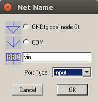
6.Provide input, output, vdd and vss pins and specify net names and port types.
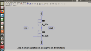
7. So finally, schematic should look like this. It will be saved in .asc format [<name>.asc].
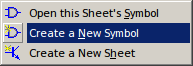
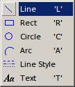
8. Next step is to create a symbol for this schematic. Go to Hierarchy –> Create a New Symbol. For creating a line in the symbol, click on Draw –> Line or L. You can also use circles and arcs for creating symbol.
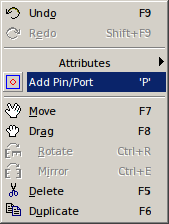
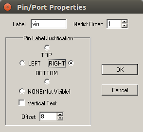
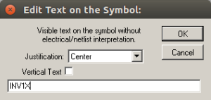
9. To add pins, go to Edit –> Add Pin Port [or P]. Give the pin name and pin justification as shown. Name can be added in symbol using T key.
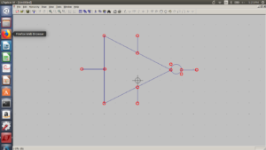
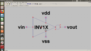
10. Final symbol should look like this. It will be saved in .asy format [<name>.asy] and can be used as a component in your schematic.
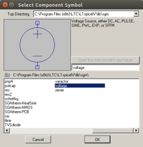
11. Now create a test file (New Schematic) to check whether our model is working or not. Select the previously created symbol from components.

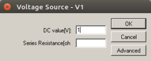
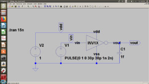
12. Select voltage source from component for input and vdd. Connect them to respective pins of symbol and specify their values as shown. Select Ground and connect to vss pin.
![]()
13. Now select the capacitor and give capacitance value and complete the connections.
![]()
14. Save it as <name_test>.asc and finally the test schematic file should look like this.
SIMULATING THE SPICE MODEL
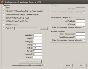
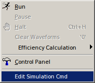
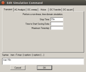
1. To simulate the Spice model, go to Simulate –> Edit Simulation cmd. Specify stop Time.
2. Now go to Simulate –> Run or click on Run icon. Now a .raw simulation window will open.
![]()
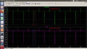
3. Select input and output net from test schematic file and respective waveforms will appear in this window. To split the waveforms, right click on the screen and select ‘Add plot pane’. Then drag one of the waveforms to empty pane.


TRANSIENT ANALYSIS
- Here we will analyse and try to find out the rise time, fall time and propagation delay of the inverter. We will also analyse their variation by changing load capacitance and input transition.
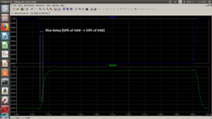
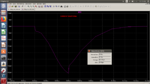
Rise Time & Fall Time:
- Rise time : Time taken by the output to rise from say 10% to 90% of vdd.
- Fall time : Time taken by the output to fall from say 90% to 10% of vdd.
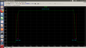
Propagation Delay:
- TpLH: Delay when output switches from low to high, after the input switches from high to low, which is measured between 50% of input & output.
- TpHL: Delay when output switches from high to low, after the input switches from low to high, which is measured between 50% of input & output.
- Propagation delay = (TpLH + TpHL) / 2.
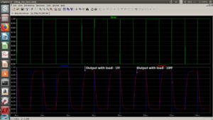
Delay variation w.r.t Load & input transition
The delay of a cell depends on output load capacitance and input transition. Cell delay increases with increase in load capacitance and input transition, as the capacitor takes more time to charge and discharge. Delay can be reduced by increasing the drive strength of the cell. As the width increases, resistance decreases, thereby increasing the current driving capability of the cell.
![]()
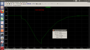
Power Calculation :-
Power can be calculated by multiplying the current (Ids) through supply voltage and vdd. First left click on wire connected to vdd to get voltage waveform. Then left click on vdd voltage source to get Ids current waveform. Right click on voltage name in the waveform. Now an expression editor opens. Write required expression to get power waveform.

The current displayed here is short circuit current which flows from vdd to vss during input transitions. To calculate average Current or Power, zoom in a particular region as shown below.
To calculate average and RMS values for current or power, press ctrl and left click on the name of respective entity. A waveform window will open which displays the average and RMS values.
A sample library designed by SignOff Semiconductors Pvt Ltd. Click to download
To be continued..
Link to #2 – https://signoffsemiconductors.com/getting-started-with-ubuntu-standard-cell-design-layout-2/ (Blog on layout using Electric)
Comments are closed.
