Pulse Width Reduction
Author : Srinivasu Rajanala, Physical Design Engineer, SignOff Semiconductors
Please read our blog on cell design to implement clock buffer.
What is the need of balanced buffers in clock path (Pulse Width Violation) ?
Balanced buffers are preferred for clock tree synthesis. If unbalanced buffers (unequal rise & fall time) are used in CTS, then pulse width reduces & minimum pulse width violation occurs.
How unbalanced buffer reduces pulse width?
Figure 1 shows the schematic of buffer with Wp = 100nm & Wn = 100nm. β ratio (the ratio of width of PMOS to width of NMOS) is not adjusted to balance rise & fall time. As mobility for NMOS is more than that of PMOS, rise time is more than fall time.
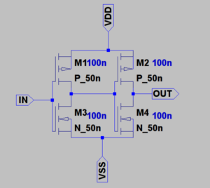
Figure 1 : Unbalanced Buffer Schematic
If we connect more number of buffers in series manner like as shown in Figure 2.
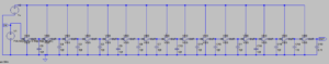
Figure 2 : Unbalanced Buffer Chain
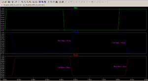
Here every buffer is taking more time to charge than to discharge. When clock signal propagates through chain of buffers, pulse width is reduced by considerable amount as shown below. Input is set as a pulse of period 4ns with 50% duty cycle. The output of last buffer has same period but duty cycle is changed. ON time of the output is reduced drastically & in worst case situation this may be less than required pulse width (minimum pulse width).
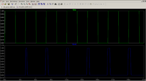
Figure 3 : Pulse Width Reduction
If PMOS width is increased more than NMOS width, after some value of β, fall time will be more than rise time. β ratio is still not adjusted to balance rise & fall time. In this case also, output of last buffer has same period but duty cycle is changed. OFF time of the output is reduced drastically & in worst case situation this may be less than required minimum pulse width (this can happen in negative edge triggered clock).
If balanced buffers are used instead of unbalanced buffers, pulse width violations can be avoided.
Balanced buffers have equal rise and fall time.
Need of balanced buffers in clock path:
For similar rise and fall time, width of PMOS should be approximately twice the width of NMOS. But exact value depends on technology.

Figure 4 : Balanced Buffer Schematic
No pulse width violation occurs when we use balanced buffers in clock path.

Figure 5 : Balanced Buffer Chain Output
Why unbalanced inverters don’t have pulse width violation :
If even number of inverters are used in clock path, pulse width will not be changed because rise and fall times will compensate each other after couple of inverters. So inverter output does not cause pulse width violation.
Figure 6 shows schematic of inverter with Wp = 100nm & Wn = 300nm. These values of Wp and Wn make rise time much less than fall time.

Fig 6 : Unbalanced Inverter Schematic
Figure 7 shows chain of unbalanced inverters and figure 8 shows the waveforms for schematic in figure 7.
Fig 7 : Unbalanced Inverter Chain
These waveforms are output of 9th and 10th inverters.
If we are using unbalanced buffers in clock path then there are chances of pulse width violation at clock pins of flip-flops. So, there will be setup and hold violation which will lead to metastability.
Hence, balanced buffers (clock buffers) are preferred in clock path.
Comments are closed.
