IC Design & Flow Overview
INTRODUCTION:
Integrated circuits (ICs) have revolutionized the world as we know it. They power the devices we use every day and have enabled advancements in fields ranging from telecommunications to medicine. But have you ever wondered how these tiny chips, no bigger than a fingernail, are designed and manufactured? The IC design process is a complex and multi-faceted one, requiring a deep understanding of both technology and engineering principles. This blog aims to provide a comprehensive overview of the IC design flow, from concept to creation. Whether you are a seasoned engineer or just starting to explore the world of IC design services , this guide will give you a comprehensive understanding of the process and its key components. So buckle up and join us on this exciting journey into the world of IC design!
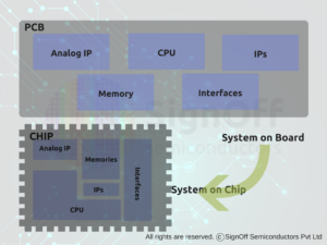
Advantages of SoC
- Compact system size (Chip size is very less compared to board size)
- Less power consumption (Less components, less IOs, less passive components helps to reduce power)
- High performance
- Less system cost
PCB – SoC
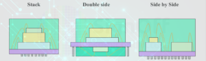
SiP (System in Package)
Advantages
- Developing cost will be less
- Faster turn around time (Development time will be less)
- Different technology chips can be mounted in same package
- Yield will be increased, as individual chip size are small
General CHIP design flow
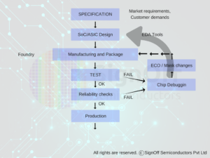
All semicon giants follow a robust SoC/IC design flow, to get reduce the TTM in this competitive market. Development cost of any SoC/IC is very high & hence every one targets for first pass silicon. A successful chip is not enough, it has to meet many criteria like Power, Performance, Area, Schedule (PPAS), Yield, Cost. All these can be achieved with systematic, flawless flow.
A general IC design flow is shown in the figure.
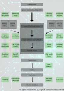
Detailed IC Design Flow
Comments are closed.