Introduction
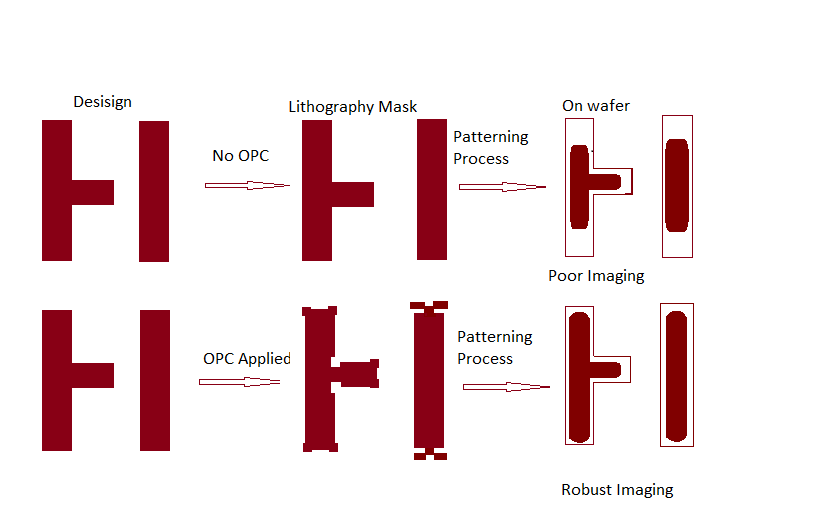
Optical Proximity Correction OPC is a resolution enhancement technique based on optical lithography. It is used in sub-wavelength lithography to deal with the severe image distortions. These image distortions typically include the: increased corner rounding, line-end shortening and changes in the width when located in isolated or dense environments. This technique helps in improving the imaging resolution. It is very important for the OPC to be efficient, especially for full-chip modification with complicated circuit layout in advanced technology nodes.
OPC is widely used in lithography for increasing the achievable resolution and pattern transfer fidelity in IC manufacturing. The OPC is based on the fundamental idea of modifying the mask itself for the correction of non-idealities that occur during the pattern transfer.
The main technique utilized to create VLSI circuits is optical microlithography. The success of this technology is attributable to the simplicity with which optical projection printing can transfer layout patterns to silicon, leading to excellent yield and throughput. These lithography advancements over the past fifteen years have significantly contributed to lowering design rules for device sizes This miniaturization effort has been motivated by the need for circuits that operate more quickly and efficiently.
With the further progress in lithography, the size of the devices could go down to 0.10 um and even below. However, we reach the limits of lithography and pattern transfer before reaching at such dimensions. The loss of image quality in optical lithography at smaller dimensions erodes the design-to-wafer fidelity on silicon. Yet, equipment costs, established production knowledge, and a tight production schedule act as conservative forces, helping in keeping the optical lithography viable in this range.
With the present outlook, optical lithography will remain an essential part of pattern transfer for both the economic and technological reasons, well into the 21st century. In order to further increase the lifetime of optical lithography, integrated circuit (IC) manufacturers are seeking for ways of enhancing resolution. The traditional way of increasing resolution and therefore shrinking dimensions can be achieved by using smaller wavelengths and better optics. However, the speed of technology development at smaller wavelengths is slower than the speed at which the designs are shrinking. Increasing resolution and/or compensating for pattern transfer non-idealities at the mask level mask engineering can be an alternative strategy to smaller wavelengths and improved illumination. The approach of making systematic modifications to mask geometries to compensate for pattern transfer non-idealities is typically called Optical Proximity Correction (OPC).
What is OPC?
OPC is the advanced mask engineering technique that can be used to increase layout-to-wafer pattern fidelity. The objective of OPC is to enhance optical characteristics by adjusting the mask. This is done by accounting for known effects that will happen during imaging or later processing by adjusting the mask geometry.
Why we need OPC?
Earlier when the Lithography was chosen as a basic process for semiconductor manufacturing, then the features were large as compared to the wavelength of light. Presently, the feature sizes are smaller as compared to the wavelength of even invisible radiation. As a result of this, the features exposed on the chip by mask do not exactly match the drawn features of the mask. As illustrated in figure below:
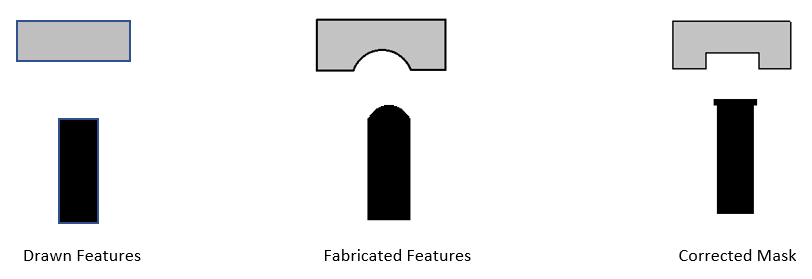
The features that are drawn on the mask result in distorted features on the wafer, this effect is called as optical proximity. The fabricated features will differ from the forms on the corrected mask, but by altering the masks, we may get the fabricated features to look the way we want them to.
Lithography
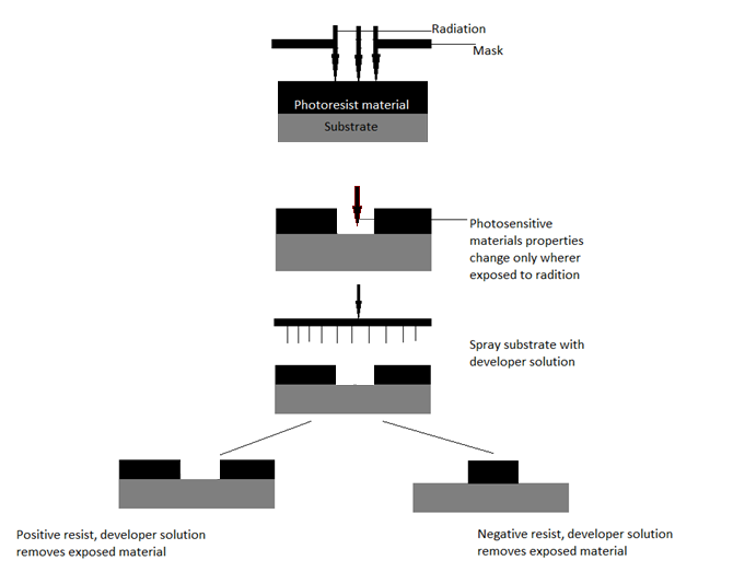
Lithography is the key technology used in semiconductor manufacturing. It is the process of transferring geometric patterns in a mask to the surface of silicon wafer. In this process, the wafer surface on which the pattern is to be transferred is covered with the radiation-sensitive material called as the resist and then it is exposed to the radiation. The radiation is transmitted through the clear parts of the mask as the exposed photoresist is insoluble in the developer solution. Then the etching process is performed to remove the unexposed portion of the wafer surface. In this way, the required geometric patterns in a mask are transferred onto the surface of the wafer.
The process of Lithography is based on the following factors:
- Resolution: – It refers to the minimum feature size; it also means the precision with which the minimum feature size can be incorporated. It depends on the wavelength of light and the numerical aperture (NA) as:
NA is proportional to Diameter of the lens/focal length
Resolution = k (λ/NA)
- Throughput: – It refers to the number of wafers that can be processed in a given time. And it is known that the bottom line is cost.
- Depth of Focus: – It is a critical factor affecting the lithography process. With the decrease in feature size, the sensitivity to focus errors increase dramatically. Depth of focus can be regarded as the range of focus errors that can be tolerated by a process along with giving acceptable lithographic results.
Optical Lithography and Its Types
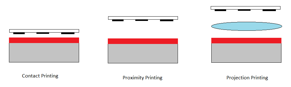
Optical lithography is the process in which the visible or ultraviolet radiation is used to transfer mask patterns onto the surface of the wafer. The masks used in optical lithography are usually made of glass or chromium.
Optical is further classified as:
- Contact printing,
- Proximity printing
- Projection printing.
- Contact printing: – It is the most widely used technique of optical lithography. In the contact printing, wafer is kept in contact with the mask, as there is no gap; this helps in achieving very high resolution. In this technique, a photomask is pressed against the resist covered wafer with pressures in the range of 0.05 atm to 0.3 atm, and is then exposed with the radiation of wavelength of about 400 nm. For providing better contact over the whole wafer 0.2mm thin flexible mask is used. And by using UV radiation, resolution size can be as low as about 1 micron.
Demerit: As the mask is in direct contact with the wafer, this significantly reduces the life of the mask.
- Proximity printing: – Proximity means close, closeness. In the proximity printing, mask and wafer are placed close to each other but they are not actually in contact, there is a small gap in between the two of them. This gap is usually in the range of 20-50 micrometers. The resolution obtained in proximity printing is low as compared to that of the contact printing. This low resolution is because of the diffraction of light that occurs as it passes through the slits. The resolution in proximity printing can be improved by reducing the gap between the mask and the wafer and by using the radiation of shorter wavelength.
Merit: – Since there is a small gap in between the mask and the wafer, this increases the life of the mask.
- Projection printing: – In the projection printing, there is a larger separation between the mask and the wafer. It involves the use of some optics and has an image formation system. The image is focused onto the wafer. Projection printers are used for printing and these printers have a well-designed objective lens between the mask and the wafer, this lens collects light from the mask and projects it onto the wafer. The capability of a lens to collect light and project it onto the wafer is measured by its numerical aperture (NA). The NA value of the lenses commonly used in projection printers typically range from 0.16 to 0.40. The resolution obtained in the process is good because of the highly focused image on the wafer. The resolution can further be improved by reducing the NA and thereby decreasing the depth of focus. While using projection printing, there is no such problem of wear and tear, and the resolution, which is obtained, is good because of the highly focused image on wafer.
Merit: – No distortion, Good resolution
Demerit – The process is costly.
Automated approaches to OPC
There have been several suggested automated OPC methods. These can be generally divided into two categories:
- Rule-based Approach
- Model-based Approach
- Rule-based Approach: –The rule-based approach performs correction of each pattern in IC layout based on the OPC rules, which are pre-determined. This rule-base stores correction values for each representative feature, which are indexed by features describing geometric information of the feature and its environment. Each of the rules has a set of crucial parameters describing the geometric information of the correction target and its environment. In order to carry out the correction, feature types are identified, geometric information parameters are evaluated, rule-base is looked upon and then accordingly the rules are applied. The geometric information parameters are evaluated based on the shape and the relative position of the correction target and its surrounding patterns. As a correction result, some small patterns are added to or removed from the original layout patterns. The pattern recognition system is used for applying the correction based on the geometric information. A particular correction is applied for a specific geometric situation, which occurs throughout the layout design.
These techniques are simple to implement, and have comparatively low cost and high throughput. These techniques are very popular in semiconductor industry and are widely applicable in several technology nodes.
- Model-based Approach: – The Model-based approach is performed by iteratively shifting the polygon edges of mask pattern until convergence requirements are achieved. And this is achieved by using a mathematical description to represent the forward model. This approach is more universal in the sense as it can be used for both 45 and 30-nm technology nodes. It is dependent upon the accurate modeling of the distortion process. This approach is further of two types as:
- Forward model-based Approach: – In the forward model-based approach, the mask pattern is parameterized by using edges and corners and then preceded by nudging these geometric elements while simulating the output wafer pattern.
- Backward model-based Approach: -In the backward model-based approach, the mathematical model is inverted and it is attempted to directly synthesize the optimized mask pattern.
Optical Proximity Correction Techniques
The Optical Proximity Correction is carried in the following ways:
- The mask pattern is divided into a number of line segments.
- And then the mask is iteratively corrected by shifting each segment independently followed by lithography simulation to check the correction result.
By these techniques, masks are analyzed and then it is determined that where the problem may occur. And based on the analysis done, the masks are modified to correct for the optical proximity effects. For the exact correction, it requires continuous curves on the masks which cannot be fabricated. There are some OPC tools, which allow the user to select the accuracy of the mask correction and also the allowable tolerance between the ideal and actual correction.
Advantages of OPC
Advantages: – OPC has the following advantages:
- With the application of OPC, more accurate critical dimensions and better edge placement can be achieved.
- OPC also has the ability to shift process windows for different types of structures, in such a way that the overlap of process windows is enlarged. This helps in more reliable pattern transfer at lower IC values.
- Tangible benefits to the IC industry include:
- Higher yield for a given minimum feature size, due to enhanced process windows.
- Better circuit performance for a given minimum feature size, due to linewidth uniformity allowing faster clock rates.
- Adoption of smaller design rules
Disclaimer:
The purpose of this blog is to spread knowledge and facilitate open discussions. The content shared is based on our research from diverse sources including the internet, books, and conversations with others. We strive for accuracy; however, we acknowledge the possibility of errors or omissions. We value your input and encourage you to share your comments, questions, and suggestions. We are open to clarifying or correcting any inaccuracies found within the blog.
Please note that while we appreciate your contributions, we may not be able to implement all suggestions. The blog should not be considered a substitute for professional advice.
Comments are closed.