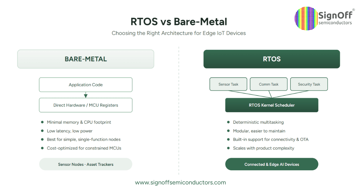
Layout Blog: Standard Cells
Multiple Architectures
Standard-cell library offers multiple architecture for best optimisation in performance, power, and area requirements of Digital designs. High Performance Architecture, a High-Density Architecture for varied customer application requirements. In each requirement (power/performance/area), layout approaches will be different to meet the design specifications. Here, we will covering in more common guidelines.
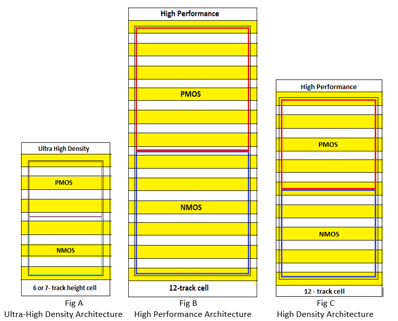
- Ultra-High Density
- Routing is complex
- Minimum area required
- Low power requirement
- High Performance Architecture
- Routing is complex compared to Ultra high density or High density architecture
- Large transistor for High speed
- Minimize power
- High Density Architecture
- Average transistor size
- Good performance
- Low power
Standard Cell Templates:
- All standard cells layout in one library follows one kind of template and it varies based on requirement.
Based on specified architecture e.g. 9T, 12T etc. Here, layer specification pre specified and need to calculate height using given data, for reference please check on below link:
Standard Cell Library – SignOff Semiconductors
Custom Architecture based on Area, Power and Performance.
These are the factors which needs to be considered while calculating standard cell height
- Maximum width for transistor
- Half DRC rules at the PR boundary: Help to decide boundary conditions
- Maximum number of pins in the single Standard cell
- Standard cell height calculation
- Tap cell: either part of standard cell layout or not
- Maximum width for transistor
- Take average size of transistor from all transistor specified in library
- Example: T1=400 nm, T2=500 nm, T3=300 nm, so average size is 400 nm.
- T2 distributed in two transistor with width of 250 nm each.
- For optimized placement and routing of transistor
- Half DRC rules at the PR boundary
- Region within which transistor placement is done, and where routing is constrained to.
- Active layer of transistor need to follow the half DRC rule at PR boundary.
- Half DRC rules means the half of the minimum rule for that particular layer.
- When abut different standard cells together there should not have any DRC violation so we have to follow half drc rules. As we can see in the below figure half DRC is maintained for poly, metals.
- It can be related to layer spacing/width/area etc and with the abutment of other cell, it will fix.

E.g. let say for metal 1 layer minimum width is 10 units than we need to keep 5 unit space from the PR boundary, So that when that logic cell abut with another logic cell not get any DRC violation.
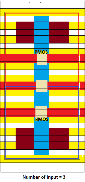
- Number of inputs
- Number of maximum input in logic cell play a vital role in calculation of Standard cell height.
- Example: NAND2x1, NOR3x1 in standard cell library. Here, need to consider maximum number of inputs while deciding the standard cell height. For this case need to consider 3 tracks.
- Consider the below example. Suppose library has maximum 3 inputs gate. In the template of standard cell we need to consider minimum 3 tracks for the input
- Standard Cell Calculation
Requirements for Standard Cell Calculation
- Calculated average with of all transistor present in the standard cell library.
Let the width is A=100 units for PMOS and NMOS
- Calculated space between active area of PMOS, NMOS and after taking required number of track for input signal.
Let the distance is B=40 units
- Calculated length of poly extended over the active layer
Let the poly extension is C= 10 units
- Calculated half DRC distance for the poly near to PR boundary
Let half DRC distance is D= 5 units
- Standard cell height = 2A + B + 2C + 2D = (2×100) + (40) + (2×10) + (2×5) = 270 unit
Also, other criterion to decide based on number of tracks, so the height of standard cell is to be multiple of metal pitch. (Here metal referred to be used at next level for the connections between standard cells pins)
- Tap cell location
- Tap cells can be added to the top and bottom
- Standard Cell Height is increases
- Mostly used for high performance standard cells
- Left and Right sides.
- The without tap cells library is preferred in high-density design.
- Standard Cell Height less compare to place at top and bottom.
- Tap cells can be added to the top and bottom
Placement of transistors, digital Block
- Use snap grid settings for faster placement of transistor and Digital layout blocks
- Set the grid according to poly pitch for placement of transistor or digital block in x-direction
- For placement and routing in y-direction follow metal pitch.
How to plan power signal and track width
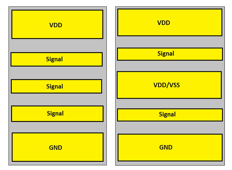
- Power/Ground:
- Power track width generally larger than minimum for reduce IR effect. Few power track examples are shown below:
- Signal:
- Try to take larger width for the output signals.
- With of metal used to make connection for the output should be more than minimum so that is get advantage of low parasitic.
- Try to take larger width for the output signals.
- Pin placement and its representation
- Pin must cover at least two Metal 2 tracks. It will be helpful in next level routing. Pin can be placed horizontally or vertically.
- How to reduce repetitive work (templates/unit cells):
- Create template
- Create set of contacts and Via’s with different enclosers.
- Create set Path and Polygons according to required min DRC
Checkout these below blog links to explore more insights on Standard Cells
- Standard Cell Library
- Getting started with Ubi, std cell design & layout #1
- Getting started with Ubi, std cell design & layout #2
Disclaimer:
The purpose of this blog is to spread knowledge and facilitate open discussions. The content shared is based on our research from diverse sources including the internet, books, and conversations with others. We strive for accuracy; however, we acknowledge the possibility of errors or omissions. We value your input and encourage you to share your comments, questions, and suggestions. We are open to clarifying or correcting any inaccuracies found within the blog.
Please note that while we appreciate your contributions, we may not be able to implement all suggestions. The blog should not be considered a substitute for professional advice.
Comments are closed.