Getting started with Ubi, std cell design & layout #2
Author : Nisha K. P., Physical Design Engineer, SignOff Semiconductors,
Author : Sumeet Anwikar, Physical Design Engineer, SignOff Semiconductors
Layout Design using free-ware tool Electric
Double click on electric to open it. A window will be displayed which will have File, Edit, Cell, Export,View, Window, Tools and Help options on the tool bar. On the left hand side pane, you will find a window which has three options namely : Layers, Components and Explorer. You will learn more about these options as we go ahead with the design.
Let us start layout designing with a CMOS inverter. To begin with, let us create a library. We need a library to organize our designs in one place.
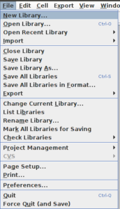
Step 1 : Create a new library
1.1 Go to File > New Library > [Library Name (say Stdcells)] > Click Ok.
1.2 Check whether the library named [Library Name (Stdcells)] is displayed on the side pane under the explorer.
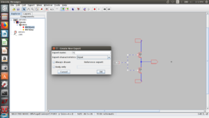
Step 2 : Create a New Cell
2.1 Right click on the newly created library Stdcells > Create New Cell (A new cell window will be displayed) > Give a cell name (say INV1X) > select schematic option from view > click OK.

2.2 Now, under the library Stdcells, you can see a cell named INV1x{sch}. The ‘sch’ in the curly braces indicate schematic view.
Step 3 : Draw the schematic of a CMOS Inverter
3.1 To design a CMOS Inverter, we need to size the PMOS and NMOS transistors. We have fixed the β ratio as 1.5. β is ratio of width of PMOS to width of NMOS. To get β = 1.5 we have taken PMOS width as 22 units and NMOS width as 15 units.
3.2 Select INV1X{sch} and click on Components. Hover the cursor over any component and its name will be displayed at the bottom of side pane.

3.3 Select the 3 terminal symbols of PMOS and NMOS and place them on schematic window. To connect two points, left click on the first point and right click on the second point. Using this technique, short the gates of NMOS and PMOS and also drains.
3.4 Double click on the PMOS, a window named Transistor properties will pop up. Change the width to 22. Similarly, change the width of NMOS to 15.

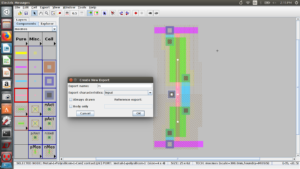
3.5 Select a Create Node: Off-page and place is at the input of the inverter. Connect this node to the shorted gates using a wire. Now select this Off-page node and press Ctrl+E. A new window named Create New Export will pop up. Give the pin name as IN under Export name and select the pin type as INPUT from the Export characteristics and click OK. You can see that the Off-page node at the input will now display ‘IN’. Similarly using Off-page nodes, give names to remaining pins i.e. VDD, VSS and OUT.
3.6 Save your inverter schematic after completion of design. To check whether the wire is properly connected or not, just click on the wire. It will highlight all the devices and pins the wire is connected to.

Step 4 : Draw the Layout of a CMOS Inverter
Before starting the layout design, please read our blog on Standard Cell Architecture for better understanding of the Layout Architecture.
4.1 To create the layout of an inverter, we need to create a new cell for layout view. Following are the steps to create a new cell for layout:
Click on the Explorer > Right click on library Stdcells > Create New Cell (A new cell window will be displayed) > Give the cell name (i.e. INV1X – cell name must be same as schematic) > select layout option from the view > click OK.

4.2 Click on Components, a list of components will be displayed under it. Hover the cursor over any component and component information will be displayed at the bottom of the side pane.

4.3 Select PMOS and place it on the layout window. Click on the PMOS gate and press Ctrl+J to rotate the PMOS. Double click on the PMOS gate. A new window titled Node Properties will appear. Change the width of PMOS to 22 units as it was in schematic.
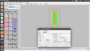
4.4 Similarly, select NMOS, rotate it and change its width to 15 units. Keep NMOS exactly below the PMOS. (Note: NMOS and PMOS should not overlap with each other)
4.5 Press F5 to check for any DRCs. If there are no error message, your design is free of DRCs. If there are some errors, close the error window and navigate to the explorer and click on errors. The errors will open a dropdown with Layout DRC(full). If you have pressed F5 multiple times, and you have received multiple error message pop ups, to recognize the current error, look for the Layout DRC(full) [current]. To avoid flooding of the errors dropdown, you can right click and select delete all to delete all the errors.
4.6 Now select pAct from components window and place it on both sides of PMOS gate. These are the source and drain contact of the PMOS. Similarly select nAct and place it on both sides of NMOS gate. These are the source and drain contacts of NMOS.
Once you place a contact, a contact need to be connected with the diffusion layer. Just like you connect two points in a schematic, here also left click on the contact and right click on the diffusion layer to connect them. Connect all the contacts to their respective diffusion layers in NMOS and PMOS. Press F5. Fix DRCs if any.
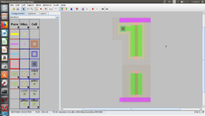
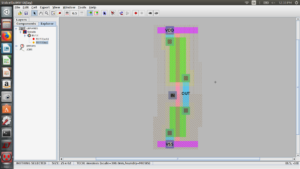
4.7 The source of PMOS is connected to VDD and that of NMOS is connected to VSS. Draw power lines using metal 1 or metal 2 at the top and bottom of layout. These are VDD and VSS lines. Connect source terminals of NMOS and PMOS to VSS and VDD respectively.
4.8 The contact left free in both PMOS and NMOS is the Drain. Move them closer and connect them.
4.9 Connect the gates of PMOS and NMOS. Select a metal to poly contact from the components and place it over the gate. Connect this contact with the gate. Press F5. Adjust the contact to fix any DRCs due to the metal to contact spacing.

4.10 Now, let us name the nodes. Click on the contact on the gate and name this contact as IN and select the contact type as Input as we did in the schematic. Similarly, name provide name to power lines as VDD and VSS. Take a metal 1 contact and place it over the drain short and name this as OUT. (Note: Names are given to contacts and pins only. Hence make sure they are provided where needed.)
Now our design is complete. Press F5. Fix DRCs if any.
Step 5 : LVS & ERC check
5.1 Navigate to Tools > NCC > Schematic and layout views of cell in the current window. If there are LVS violations, you will get an error message. Fix them appropriately. If no error messages pop up, that means LVS is clean. (Note: Before starting the LVS check, ensure that all the connections, MOS dimensions and pins are matching in both layout and schematic.)
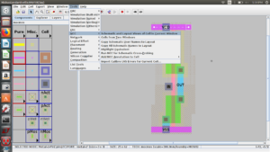

5.2 To check ERCs, we need to do body biasing for NMOS and PMOS. To do this, take nwell and place it adjacent to the PMOS at minimum distance. Press F5 and fix DRCs if any. Connect this nwell contact to VDD. Thus PMOS body is connected to VDD. Similarly, keep pwell adjacent to NMOS and connect it to VSS. Now the NMOS body is connected to VSS. Press F5 and clear DRCs if any. Once the body biasing is done, check ERCs. Navigate to Tools > ERCs > Check wells. Fix ERCs if any.

Once the DRC, LVS and ERC checks are clean, we are good to go with the design.
Guidelines to create an optimized layout:
- Draw the VDD and VSS rails at the initial stage of the layout design, say after placing the transistors. This will define the area available for further design.
- Vary the size of contacts just the way you sized PMOS and NMOS. This will help you design layouts with optimized area.
Avoid poly-bending in your layout as much as possible. Vertical poly-to-poly connections are allowed. - When you design larger layouts such as DFF, no need to give body biasing for each transistor separately. You can save area by giving common body biasing.
- In a large layouts, intermediate cells can be of optimum size but the driver should be large enough to provide the required drive strength. You will understand this better when you start designing layouts of circuits like transmission gate.
Comments are closed.
