Power is one of the most concerned factor in the lower node technologies due to sophisticated operation of a system at higher frequencies, complex functionalities, wireless applications and portability. Power dissipation has become one of the critical issues as it results in heating up of the device which in-turn affects the operation of a chip. There are many kinds of external heat sinks and software based methods are provided with the system, but we have scope to save the power during operation of the chip. Saving power is eco-friendly and improves the life time of the system.
Before going to power saving techniques, lets look at the reasons for power dissipation in MOSFET based design. The power dissipation is classified in two categories:
- Static power dissipation
- Dynamic power dissipation
1. Static power dissipation:
In this class, power will be dissipated irrespective of frequency and switching of the system. It is continuous and has become more dominant at lower node technologies. The structure and size of the device results in various leakage currents. Few reasons for static power dissipation are :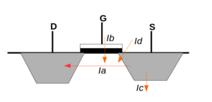
a. Sub-threshold current
b. Gate oxide leakage
c. Diode reverse bias current
d. Gate induced leakage
Its hard to find the accurate amount of leakage currents but it mainly depends on supply voltage (VDD), threshold voltage (Vth), transistor size (W/L) and the doping concentration.
2. Dynamic power dissipation:
There are two reasons of dynamic power dissipation; Switching of the device and Short circuit path from supply (VDD) to ground (VSS). This occurs during operation of the device.
a) Short-circuit power dissipation:
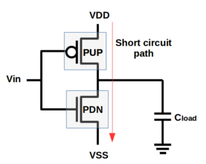 Because of slower input transition, there will be certain duration of time “t”, for which both the devices (PMOS and NMOS) are turned ON ( Vtn to VDD-Vtp ). Now, there is a short circuit path from VDD to VSS. This short circuit power is given by:
Pshort-circuit = Vdd. Isc. t
where, Vdd – Supply voltage, – Short-circuit current,
b) Switching power dissipation:
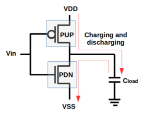 This is the power dissipated during charging and discharging of total load [output capacitance + net capacitance + input capacitance of driven cell(s)]. The switching power is given by:
Pswitch = α·VDD2 · Cload·f
where, α – Switching activity factor, f – Operating frequency,
VDD – Supply voltage & Cload – Load capacitance
Common power reduction methods are:
- Reduce VDD, Cload, f, α
- Multi voltage design.
- Multi Vth cells (LVT, RVT, HVT cells etc).
- Cells with different drive strengths.
- Dynamic Voltage & Frequency Scaling (DVFS).
- Clock gating (switching power reduction).
- Multi-track cells can be used in a design.
- Multi-bit flipflops can be used.
The power management techniques will start from the design specification stage, and are employed at each and every step of physical design flow. The below chart shows overview of power consumption at each stage.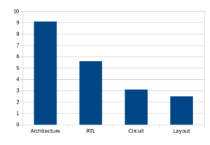
A design has sub-systems with various functionalities. While operating the system, the sub-functional blocks that are not necessary to function at a particular duration of time can be turned OFF. Similarly blocks that do not require high speed of operation can be slowed down by reducing the supply voltage. Some time, the sub-system’s functional performanance requirement varies from time to time (DVFS). All these power reduction methods add complexity to the design.
UPF provides a universal low power design specification, usually written in Tcl language. The technique primarily focuses on dynamic power consumption (which is dominant at 90nm). Here comes the requirement of multi voltage designs (which requires level shifers between different voltage domains)
As technology shrinks below 90nm, static power consumption has also become prominent. Here comes the requirement of power gating (which requires isolation cells to isolate a switching domain from an always on domain.)
To control all these, a power management unit is used, which triggers control signals of low power cells as per requirement.
The logical intent of the design is completely provided with the help of RTL code but its complicated to provide power information. Hence the power intent of the design is specified in UPF. Power management file will be built at the architecture level of design stage. This forms a complete description of the design. Various methods used for the power management are:
- Clock gating method (ICG) [logic intent of the design]
- Multiple height cells
- Multi-voltage design (MVD)
- Power shut-off (PSO) or Power Gating
- Multi-Vth design (MV)
- Dyamic voltage and frequency scaling (DVFS)
1. Clock gating method:
It is logical intent of the design which is provided in RTL code. Suppose there are a group of flops meeting “min_bit_width”, having same load enable (data to these flops are constant), clock switching can be disabled during that time, thereby saving dynamic power to a great extent. Clock is made available only when the data changes. Clock gating is implemented using an ICG cell. Read more on clock gating in our synthesis blog.
2. Multi-Voltage design:
As per the equation P = α C V2 f , as supply voltage is scaled down, power reduces to a great extent. Hence sub-systems that do not require higher speed of operation, can be operated at lower voltages, saving dynamic power. The design can have multiple voltages as per the performance requirement.
Sub-systems that operate at different voltages have separate power domains, each having separate supply ports and nets. This technique requires level shifter when a signal is passed from one domain to another, based on requirement. There are two types of level shifters:
- Low to high
- High to low
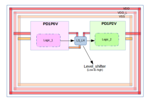 Whenever signal from low domain goes to high domain as input, there will not be full output swing available at the output of high domain. This is because signal from low domain changes the region of operations of devices in high domain. So, Low-to-high level shifter is used.
Whenever signal passes from high to low domain, if the destination cell cannot withstand high voltage, then a H-L level shifter is inserted in that path. The level shifter can be in placed in source/ destination power domain or in default domain and it will take both the voltages (source domain voltage and destination domain voltage) for its operation.
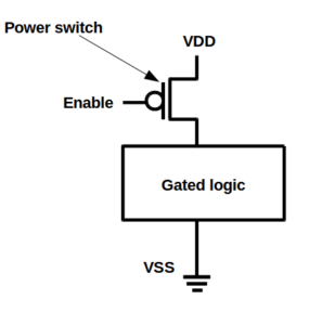
3. Power Gating :
Whenever operation of sub-blocks are not required, there is a scope to shutdown voltage domains. This technique uses power switches to disable power. The power switches are MTCMOS. During normal operation, LVT is used (to reduce short circuit power) and during off mode, HVT is used (to reduce leakage power). Power switches are controlled by the power management unit.
If the load is more, huge amount of in-rush current flows, to charge the internal capacitors. To reduce this, the power switches are enabled in a daisy chain fashion.
Isolation Cell :
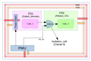 When a source domain (PD1) is in off-mode then its output pin has to be isolated from destination domain (PD2) to prevent invalid logic being propagated to PD2. Along with isolation it will save the short circuit power dissipation at the reciever cell.
There are 2 types of isolation cell as per logic requirement:
- “Clamp to 0” cell (AND gate)
- “Clamp to 1” cell (OR gate)
Retention Flop :
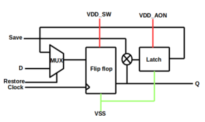 Whenever a gated domain is turned off, the state of the flop needs to be retained with less leakage power. When gated domain is powered back on, the stored data can be used, rather than initializing again.
This is achieved by using data retention flops. Retention flops contains a DFF and latch. It requires low power always-on supply to retain the data.
This feature comes with the cost of Area of the device which is more compared to normal flop and An aditional power supply has to be provided which is low-voltage always ON.
Always ON cell :
Always on cells are special cells which are always turned-on irrespective of their placement in switching domain. They are used to drive the net which is passing from always on domain. Generally Always-ON buffers and inverters are used. We need to define the always on cells in the UPF file.
4. Multi-Vth design (MV)
In a design, standard cells are provided with different flavors based on the threshold voltage. Variation in threshold voltage will affect the power consumption and timing hence these are used to optimize the power and timing issues. These cells are usually named as:
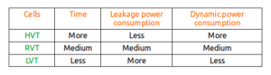
- HVT cells
- RVT cells
- LVT cells
This table shows the characteristics of Multi-Vth cells. The area of all the flavours of a cell is always same. Only threshold voltage varies and hence power and delay.
The design is synthesized with RVT and HVT cells but while optimizing LVT cells are used to meet the critical timing issues.
5. Dyamic voltage and frequency scaling (DVFS)
This method is used to vary the voltage and frequency based on requirement. The voltage and/or frequency of the design can be scaled as per performance requirement.
An advance method AVFS has been introduced where the feedback is provided to controller to decide voltage and/or frequency but it is very complex.
Example: Consider the following design.
This design consists of default with three different voltage domains APD1P2V, SPD1P0V and APD0P8V.
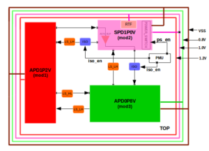
- APD1P2V – Always on power domain with 1.2V supply
- SPD1P0V – Switching power domain with 1.0V supply
- APD0P8V – Always on power domain with 0.8V supply
- LS_LH – Level shifter low to high
- LS_HL – Level shifter high to low
- ISO – Isolation cell
- RTF – Retension Flop
- PMU – Power management unit
- AON_BUF –Always on buffer
There are various commands provided to specify UPF completely and it can be easily understandable by command itself, few of which are explained here to write UPF of above example.
upf_version : As UPF have been modified stage by stage, it has different versions. So its necessary to provide version of upf being used to interpret the upf commands.
upf_version [string]
The version can be 1.0, 2.0 etc.
Power Domain (PD) : A set of modules using a same voltage belongs a power domain. The command “create_power_domain” is used to define a power domain and its characteristics.
UPF for the above Power Intent:
#———- Create Power Domains ————–#
create_power_domain TOP -include_scope
create_power_domain APD1P2V -elements { TOP/mod1 }
create_power_domain SPD1P0V -elements { TOP/mod2 }
create_power_domain APD0P8V -elements { TOP/mod3 }
#——– Supply Ports & Net Connections ————#
create_supply_port VDD1P2
create_supply_net VDD1P2 -domain TOP
create_supply_net VDD1P2 -domain APD1P2V -reuse
connect_supply_net VDD1P2 -ports VDD1P2
create_supply_port VDD1P0
create_supply_net VDD1P0 -domain TOP
create_supply_net VDD1P0 -domain SPD1P0V -reuse
create_supply_net VDD1P0_SW -domain SPD1P0V #switching net
connect_supply_net VDD1P0 -ports VDD1P0
create_supply_port VDD0P8
create_supply_net VDD0P8 -domain TOP
create_supply_net VDD0P8 -domain APD0P8V -reuse
connect_supply_net VDD0P8 -ports VDD0P8
create_supply_port VSS
create_supply_net VSS -domain TOP
create_supply_net VSS -domain APD1P2V -reuse
create_supply_net VSS -domain SPD1P0V -reuse
create_supply_net VSS -domain APD0P8V -reuse
connect_supply_net VSS -ports VSS
#———- Establish Connection ————-#
set_domain_supply_net TOP -primary_power_net VDD1P0 -primary_ground_net VSS
set_domain_supply_net APD1P2V -primary_power_net VDD1P2 -primary_ground_net VSS
set_domain_supply_net SPD1P0V -primary_power_net VDD1P0 -primary_ground_net VSS
set_domain_supply_net APD0P8V -primary_power_net VDD0P8 -primary_ground_net VSS
#———- Shut-down Logic for Reciever ————#
create_power_switch POWER_SWITCH -domain SPD1P0V \
-input_supply_port {VDD1P0 VDD1P0}\
-output_supply_port { VDD1P0 VDD1P0_SW} \
-control_port {PMU/ps_en } \
-on_state {state_name VDD1P0 {!ps_en}}
#———- Isolation Cell Setting ———–#
set_isolation iso_out -domain SPD1P0V \
-applies_to outputs \
-isolation_power_net VDD1P0 -isolation_ground_net VSS \
-clamp_value 1 \
-isolation_signal PMU/iso_en \
-location default
#———– Retention Logic for SPD ———-#
set_retention RTF -domain SPD1P0V \
-retention_power_net VDD1P0 \
-retention_ground_net VSS \
-save_signal {PMU/rtf_en high} \
-restore_signal {PMU/rtf_en low} \
#——– Level Shifter for multi-VDD Domain ———#
set_level_shifter LS_0P8_1P0 -domain SPD1P0V \
-applies_to inputs \
-location self \
-source APD0P8V.primary \
-input_supply_set APD0P8V.primary -output_supply_set SPD1P0V.primary
set_level_shifter LS_1P0_1P2 -domain APD1P2V \
-applies_to inputs \
-location self \
-source SPD1P0V.primary \
-input_supply_set SPD1P0V.primary -output_supply_set APD1P2V.primary
set_level_shifter LS_1P2_0P8 -domain APD0P8V \
-applies_to inputs \
-location self \
-source APD1P2V.primary \
-input_supply_set APD1P2V.primary -output_supply_set APD0P8V.primary
set_level_shifter LS_0P8_1P2 -domain APD0P8V \
-applies_to inputs \
-location self \
-source APD0P8V.primary \
-input_supply_set APD0P8V.primary -output_supply_set APD1P2V.primary
#———– Define Always ON Cell ————-#
define_always_on_cell -cells AON_BUF \
-power_switchable VDD1P0_SW -ground_switchable VSS \
-power VDD1P0 -ground VSS
#——— Create Power State Table ———–#
add_power_state TOP.primary \
-state ON { -supply_expr {power == ‘ {FULL_ON, 1.0} && ground == ‘ {FULL_ON, 0.0 }} \ -simstate NORMAL }
add_power_state APD1P2V.primary \
-state ON { -supply_expr {power == ‘ {FULL_ON, 1.2} && ground == ‘ {FULL_ON, 0.0 }} \ -simstate NORMAL }
add_power_state SPD1P0V.primary \
-state ON { -supply_expr {power == ‘ {FULL_ON, 1.0} && ground == ‘ {FULL_ON, 0.0 }} \ -simstate NORMAL }
-state OFF { -supply_expr {power == ‘ {OFF} && ground == ‘ {FULL_ON, 0.0 }} \
-simstate CURRUPT }
add_power_state APD0P8V.primary \
-state ON { -supply_expr {power == ‘ {FULL_ON, 0.8} && ground == ‘ {FULL_ON, 0.0 }} \
-simstate NORMAL }
Comments are closed.
