SignOff checks
Author : Aglow A George, Physical Design Engineer, SignOff Semiconductors
Author: Batchu Sri Sai Chaitanya, Physical Design Engineer, Signoff Semiconductors
Author: Ashish Kumar Sharma, Physical Design Engineer, Signoff Semiconductors
Design Rule Check (DRC)
Design Rule Check (DRC) determines whether the layout of a chip satisfies a series of recommended parameters called design rules. Design rules are set of parameters provided by semiconductor manufacturers to the designers, in order to verify the correctness of a mask set. It varies based on semiconductor manufacturing process. These rule set describes certain restrictions in geometry and connectivity to ensure that the design has sufficient margin to take care of any variability in manufacturing process.
Design rule checks are nothing but physical checks of metal width, pitch and spacing requirement for the different layers with respect to different manufacturing process. If we give physical connection to the components without considering the DRC rules, then it will lead to failure of functionality of chip, so all DRC violations has to be cleaned up.
After the completion of physical connection, we check each and every polygon in the design, based on the design rules and reports all the violations. This whole process is called Design Rule Check.
Typical DRC rules are:
- Interior
- Exterior
- Enclosure
- Extension
Interior:

Fig1: Distance of interior facing edge for a single layer.

Fig2: Distance of interior facing edge of two layer.
Exterior:
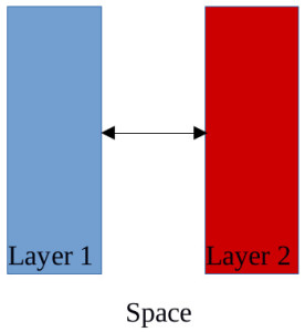
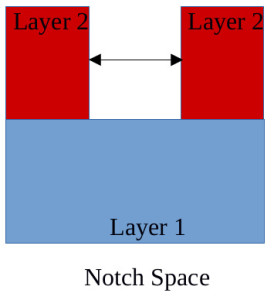
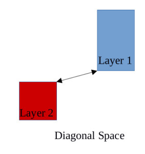
Fig3: Distance of exterior facing edge of two layer
Enclosure:
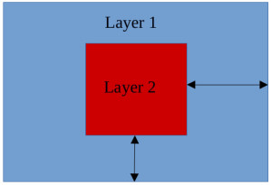

Fig4: Distance between inside edge to outside edge.
Extension:
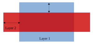
Fig4: Distance between inside edge to outside edge.
To understand the basic design rules, let’s take CMOS inverter as an examples:

Fig5: CMOS Inverter layout

Layout versus Schematic (LVS)
DRC only verifies that the given layout satisfies the design rules provided by the fabrication unit. It does not ensure the functionality of layout. Because of this, idea of LVS is orginated. This blog focuses on how LVS works and what all are the common issues faced in LVS.
How LVS works
Inputs needed to perform LVS are:
- .v – netlist of the design
- GDS – layout database of the design
- LVS rule deck
.v and GDS should be of same stage.
LVS rule deck is a set of code written in Standard Verification Rule Format (SVRF) or TCL Verification Format (TVF). It guides the tool to extract the devices and the connectivity of IC’s. It contains the layer definition to identify the layers used in layout file and to match it with the location of layer in GDS. It also contains device structure definitions.
LVS check involves three steps:
- Extraction: The tool takes GDSII file containing all the layers and uses polygon based approach to determine the components like transistors, diodes, capacitors and resistors and also connectivity information between devices presented in the layout by their layers of construction. All the device layers, terminals of the devices, size of devices, nets, vias and the locations of pins are defined and given an unique identification.
- Reduction: All the defined information is extracted in the form of netlist.
- Comparison: The extracted layout netlist is then compared to the netlist of the same stage using the LVS rule deck. In this stage the number of instances, nets and ports are compared. All the mismatches such as shorts and opens, pin mismatch etc.. are reported. The tools also checks topology and size mismatch.

Fig6: LVS Flow
Commonly faced LVS issues:
LVS check includes following comparisons:
- Number of devices in schematic and its layout
- Type of devices in schematic and its layout
- Number of nets in schematic and its layout
Typical errors which can occur during LVS checks are:
- Shorts: Shorts are formed, if two or more wires which should not be connected together are connected.
- Opens: Opens are formed, if the wires or components which should be connected together are left floating or partially connected.
- Component mismatch: Component mismatch can happen, if components of different types are used (e.g, LVT cells instead of HVT cells).
- Missing components: Component missing can happen, if an expected component is left out from the layout.
- Parameter mismatch: All components has it’s own properties, LVS tool is configured to compare these properties with some tolerance. If this tolerance is not met, then it will give parameter mismatch.
IR Drop Analysis:
IR Drop can be defined as the voltage drop in metal wires constituting power grids before it reaches the vdd pins of the cells. IR drop occurs when there are cells with high current requirement or high switching regions. IR drop causes voltage drop which in-turn causes the delaying of the cells causing setup and hold violations. Hold violations cannot be fixed once the chip is fabricated.
There are two types of IR drop analysis namely:
Static IR drop analysis:
- Calculates the average voltage drop of entire design assuming current drawn across is constant.
- As average current is calculated this analysis depends on time period. This analysis is good for signoff checks in older technology.
Dynamic IR drop analysis:
- Depends on switching activity of the logic.
- Is vector dependent .
- Less dependent on clock period as depends on instantaneous current.
- Analysis of peak current demand and highly localized cells.
Methods to reduce IR drop:
-
Robust power mesh– Initial power grid is made based on static ir analysis due to late availability of switching activity. If there is IR drop due to some of the clustered cells then adding a strip will make the power mesh more robust.
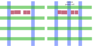
Fig7: Custom power rail added to make it robust
-
De-cap– These are decoupling capacitors which are spread across the high switching region to maintain the voltage.
-
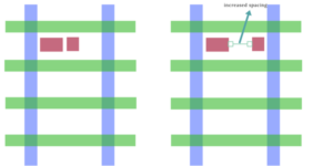
Spacing– If clock cells are clustered and causing IR drop, then by spacing them apart near to different power rails will reduce the IR drop. While shifting the cell to next power rail, it should be made sure that the power rail is not driving many cells, because adding another cell may give IR drop.
-
Reducing load– Cells driving more load will be drawing more current. Hence reducing load will reduce IR drop.
-
Downsizing– Cells of smaller size will draw less current. But the transition of cells should not become worse.
-
The number of power switches can be increased to reduce IR drop
-
It should be made sure that all the power pins of macros are properly connected to the power rails.
Note:
- For accurate dynamic analysis vcd files (switching activity file) with sdf (standard delay format) is better.
- Glitches produced from combinational circuit may act as instantaneous switch. Reducing them will decrease the pessimism of dynamic IR drop analysis.
- IR drop analysis is done in RC worst corner (corner having more resistance of rails) and FF process, high voltage and high temp corner (PVT corner) because current is drawn more in this corner.
ELECTRO MIGRATION (EM):
Electro migration (EM) refers to the unwanted movement of materials in a semiconductor. If the current density is high enough, there can be a momentum transfer from moving electrons to the metal ions making the ions to drift in the direction of the electron flow. This results in the gradual displacement of metal atoms in a semiconductor, potentially causing open and short circuits. Due to high current density and resistance of metal in the recent technologies EM has become dominating.
- EM leads to open circuits due to voids in wires or vias and leads to short circuits due to extrusions or “hillocks” on wires. Either can cause a system failure that is hard to diagnose.
- During older technology nodes EM was considered only on power wires and clock wires. But now signal wires also need to be considered due to increased current density in them.
- Fin-FETs have more current density than planar transistors, thus making EM worse, especially in conjunction with narrow wires.
- Copper interconnects worsen EM because the copper molecule moves faster.
- In the recent technologies the lower supply voltages is helping to reduce EM, but not enough to offset all the other causes that amplify it.
- EM is worse at higher temperatures.
- EM fixing techniques such as widening wires, can increase area and cause timing violations. EM fixing needs to be timing-driven.
Methods to fix EM
- Widen the wire to reduce current density
- Keep the wire length short
- Reduce buffer size in clock line
Not in PD point of view
- Reduce the frequency
- Lower the supply voltage
SCAN Tracing:
Files (Scan DEF and .V)
In scan tracing we are checking the connection of flip flops, there should not be any floating connections. The reason why we are doing scan tracing is because, in formality check we disable the Scan(so it doesn’t check the scan chain), and we are assuring that there is no issue with scan chains.
DFM:
Files (GDS and Rule deck file)
As the technology scales down, manufacturing process is becoming more complex. DFM (design for manufacturing) is the stage in which we modify or add extra things (like redundant via insertion, wire spreading). These techniques will increase the yield and reliability in the design.
Few DFM steps:
- Redundant Via insertion.
- Wire spreading.
- Wire slotting.
- Metal filling.
Formality Check:
Files (Reference netlist, Implemented Netlist, .V and .Lib)
The basic idea behind FM check is to compare implemented netlist with reference netlist (Synthesis stage netlist / golden netlist). We check whether the logic output value given in both stages are same.
Example 1: If we check the FM in the Scan mode (i.e, in ON state) we will get the formality issues, because during the scan chain reordering the position of Flip Flops will be changed with respect to SCAN def file. To overcome this issue, we have to disable the scan port (by assigning it’s value to “0”).
Example 2: Undriven port Issue: In golden netlist for the floating pins binary values are assigned like “0” or ”1”, but when it gets implemented floating pin is assigned as “X ” which leads to mismatch. To resolve this issue, we set both pins in implemented and reference netlist either “0” or “1”.
Power Analysis:
Files (SPEF, SAIF,.V, Lib, UPF and SDF)
In Power analysis we calculate the power dissipation. Two types of power dissipation, (i) Leakage Power (ii) Dynamic power. Leakage power is basically static power which is dissipate during the Off state or non-toggling (when the input data is fixed) state of device, and for the dynamic power the activity factor is required, which is present in the SAIF (switching activity interchange format) file. We also check for hot spot in the design, the hot spot is basically the small region where the higher power dissipation is present.
Comments are closed.
