Silicon On Insulator ( SOI )
Author : Abhishek Kumar, Physical Design Engineer, SignOff Semiconductors
Author: Ankit Varma, Physical Design Engineer, Signoff Semiconductors
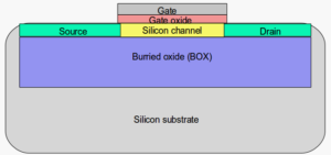
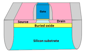
Silicon on insulator (SOI) refers to the use of a three layered substrate in place of conventional bulk silicon substrates. A thin layer of silicon is placed on top of an insulator such as silicon dioxide (SiO2) also known as a buried oxide layer. This layer lies upon the substrate and isolates the body from the substrate. The transistors are then built upon the thin silicon layer. The full dielectric isolation of the devices reduces parasitic capacitance, thereby improving performance.
The choice of the insulating layer depends largely on the intended application. Sapphire is used for high performance radio frequency (RF) and Radiation sensitive applications & SiO2 is used for diminished short channel effects in microelectronic devices.
What is the need of SOI ?
- For the continuation of Moore’s Law beyond 28 nm with an upgrade to traditional planar bulk CMOS technology.
- Increased complexities in scaling of conventional bulk CMOS technology.
- To avoid interactions between the devices and the substrate which gives rise to unwanted parasitic effects, mainly the parasitic capacitance developed between diffused source and drain and the substrate.
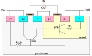
- To prevent latchup, which is the generation of a low impedance path between the Vdd & Vss rails due to formation of parasitic pnp and npn Bipolar Junction Transistors in a bulk CMOS process. These BJTs form a pnpn structure with positive feedback and virtually short-circuit the power rail to ground, thus causing excessive current flows and even permanent device damage.
- The full dielectric isolation of the devices reduces parasitic capacitance, thereby improving performance. To overcome short-channel effects inherent to sub-micron devices.
- As transistor shrinks, the length of the gate is reduced. The control of the gate over a channel region is also reduced, thus lowering the transistor performance. SOI provides more control over channel using body biasing.
- To reduce the growing leakage power due to subthreshold leakage and diode leakage currents.
- To reduce manufacturing complexity while continuing to deliver high perfomance at lower cost and with lower power consumption.
Types of SOI devices
There are two different types of SOI devices:
1. Partially Depleted Silicon On Insulator (PD-SOI)
In a PDSOI N-type MOSFET, top silicon layer is thicker and the holes are pushed toward the buried oxide layer creating a region called floating body, which can store charge. That creates a modified switching threshold point, which depends on the history of the circuit. The inversion region does not extend the full depth of the body leaving a floating body in the channel. The insulating buried oxide layer is also thicker and channel is doped. The partially depleted SOI device behaves similarly to the bulk device, except that charge can accumulate in the body and modify its characteristics.Simpler technology with no wells and trenches.
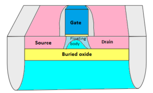
- Insulated BOX layer is of thickness 100-200 nm
- Top silicon layer is 50-90 nm
- Used in analog circuits
- Doped channel
Problems associated with PD-SOI
- History effect– The body of the NMOS or PMOS Transistors in the PD-SOI is floating instead of being tied to Vss for nmos or Vdd for pmos as in bulk CMOS. Due to the differences in the body voltages, threshold voltage can change. This could cause delay variations and mismatch between two identical devices. As the SOI circuit switches, the body Voltages of the switching transistors will change from their previous steady state condition. This is called the history effect. The exact voltage depends on the history of source, gate, and drain voltages leading up to the current time. The body voltage affects the conduction of the channel and therefore the switching speed and parasitic capacitance of the circuit.
- PD SOI MOSFETs require high channel doping to suppress short-channel effects.
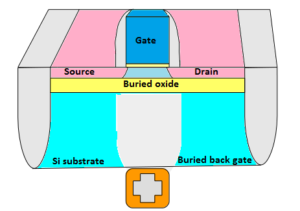
2. Fully Depleted Silicon On Insulator (FD-SOI)
FD-SOI is a planar process technology with two major changes made in bulk CMOS technology. First, an ultra-thin layer of insulator, called the buried oxide, is placed on top of the base silicon substrate. Then, a very thin silicon film placed on top of insulating layer implements the pmos and nmos devices. Silicon layer under the gate is so thin that it is fully depleted of mobile charge carriers and no doping is required in the channel. when the channel is very lightly doped and very thin, the depletion region fills the full length of the body, thus eliminating the floating body region. The combination of these two innovations is called “ultra-thin body and buried oxide Fully Depleted SOI” or UTBB-FD-SOI.
- The insulating buried oxide layer lowers the parasitic capacitance between the source and drain and the substrate.
- The insulator layer efficiently confines the flow of electrons from source to the drain, drastically reducing the performance degrading leakage currents from the channel to the substrate.
- Faster operation at lower voltage and better power management. Body biasing is more effective for controlling the transistor channel because of an ultra-thin buried oxide.
- Insulated BOX layer is of thickness 5-50 nm.
- Top silicon layer is 5-20 nm.
- Used in low power applications.
- Undoped channel.
Body Biasing: In order to improve transistor performance a voltage can be applied to the substrate. This method called body biasing or back biasing facilitates the creation of the chaannel between the source and the drain resulting in faster switching of the transistor.
In bulk CMOS, body biasing is very limited due to leakage current and reduced transistor geometry. Because of the ultra thin insulator layer in FD-SOI, the body biasing creates a buried gate below the channel making the FD-SOI act like a vertical double gate transistor.
Different voltages can be applied to the top and buried gates which effectively changes the characteristics of the transistor. FD-SOI can be made to work in either high performance mode or low power mode based on the voltages applied on top and buried gates.
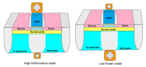
- The buried gate prevents any leakage in the substrate and allows much higher voltage on the body leading to boost in performance.
- FD-SOI shows improved power efficiency, lower thermal dissipation, and extended battery life for portable devices.
- It is able to operate at lower voltage than bulk CMOS while giving better performance. This makes FD-SOI chip cooler with lower power consumption.
- In FD-SOI, dopant usage is greatly reduced thus limiting the process variations.This allows the transistor to operate faster for a given voltage, since less margin is allowed for process variability.
- FD-SOI is a planar technology that re-uses most of the processing steps used in bulk CMOS process. Overall manufacturing process in FD-SOI is less complex, leading to reduced manufacturing cost and lower cycle time.
- Allows smaller and simpler analog circuits, with higher performance at lower operating power due to the absence of channel doping and well implants in the FD-SOI.
Many techniques have been used in producing the SOI materials:
- Homoepitaxial techniques
- Heteroepitaxial techniques
- Recrystallization techniques
- SIMOX (Separation by IMplanted Oxygen)
- FIPOS (Full isolation by oxidized porous silicon)
- Unibond
- Eltran
- Wafer Bonding
CMOS fabrication by SOI technology:-
The subsequent steps for fabrication of CMOS SOI are similar to Bulk Technology.
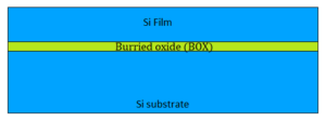
Fig1: SOI structure
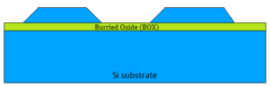
Fig2: Island formation
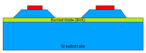
Fig3: Poly Si gates
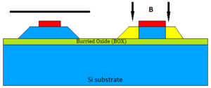
Fig4: P+ drain / source
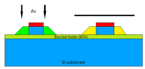
Fig5: N+ drain / source
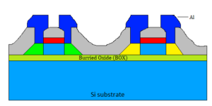
Fig6: Metallization
Advantages of SOI over bulk CMOS process:-
- Better electrostatic control of the channel.
- Reduction of parasitic junction capacitances.
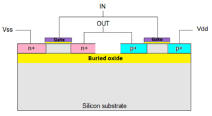
- Excellent latchup immunity because of buried oxide layer.
- Limited short channel effects compared to bulk CMOS technology.
- Reduced subthreshold leakage and diode leakage.
- Higher speed and lower power consumption.
- Gives high-performance and cost-effective alternative to bulk CMOS technology.
- Smaller transistor saves lot of area and provides higher packaging density.
- Radiation tolerance – Reduced soft error rates, which refers to change of data in the memory for space application because of radiations.
- Involves fewer manufacturing and processing steps than bulk CMOS technology.
- Simpler technology with no wells and trenches.
- Substrate noise is reduced because the burried oxide layer acts as a dielectric barrier.
Problems:
- Self-heating due to the low thermal conductivity of the buried oxide.
- History effect (Floating body effect) in PD-SOI.
- Difficulty in manufacturing thin body SOI wafers in FD SOI.
Comments are closed.
