CMOS technology uses both NMOS and PMOS transistors, The transistors are arranged in a structure formed by two complementary networks. Bulk CMOS is a chip built on a standard silicon wafer.
Fabrication steps of Bulk CMOS
The fabrication of Bulk CMOS has following steps:
- Create an n-well region and channel stop regions.
- Grow field oxide and Gate oxide.
- Deposit and pattern Polysilicon layer.
- Implant sources, Drains and the substrate contact regions.
- Create contact windows, Deposit and pattern metal layer.
The fabrication of CMOS requires six mask set they are:
- n well or P well (Depends on process).
- Polysilicon.
- n+ diffusion.
- P+diffusion.
- Contact.
- Metal.
There are a number of approaches to CMOS fabrication p-well, n-well, and the twin-tub process. CMOS can be obtained by integrating both the NMOS and PMOS transistors on the same chip substrate. For integrating these NMOS and PMOS devices on the same chip, special regions called as wells or tubs are required in which semiconductor type and substrate type are opposite to each other. A P-well has to be created on an N-substrate or N-well has to be created on a P-substrate. In the subsequent steps, the fabrication of CMOS is described using the P-substrate in which the NMOS transistor is fabricated on a P-type substrate and the PMOS transistor is fabricated in n-well.The n-well process is widely used.
The process begins with the creation of an n-well on a bare type silicon wafer. Fig 1 shows a bare substrate before processing.

Figure 1: Bare silicon wafer (p type)
In the region of the well group V dopants are added into the silicon substrate to change the substrate from p-type to n-type in the region of the well. To define this region grow a protective layer of oxide over the entire fiber and remove the protective layer where n-well is needed. The wafer is first oxidized in a high temperature typically around 900 degree Celsius to 1200 degree Celsius. Furnace causes Si and O2 to react and become SiO2 on the wafer surface as shown below.

Figure 2: Oxidation
The oxide must be patterned to define the n-well, Develop a photoresist layer on top of the oxide layer as shown in Fig.3
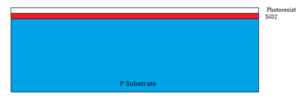
Figure 3: Photoresist
Photoresist:– A photoresist is a light-sensitive material loses its resistance or its susceptibility when it is exposed to light. It is used in several processes, such as photolithography and photoengraving, to form a patterned coating on a surface.
There are two types of Photoresist:
- Positive Photoresist.
- Negative photoresist.
Positive Photoresist:-A positive photoresist is a type of photoresist in which the portion of the photoresist that is exposed to light becomes soluble to the photoresist developer. The unexposed portion of the photoresist remains insoluble to the photoresist developer.
Negative Photoresist:– A negative photoresist is a type of photoresist in which the portion of the photoresist that is exposed to light becomes insoluble to the photoresist developer. The unexposed portion of the photoresist is dissolved by the photoresist developer.
Here Positive Photoresist is used and the light source is UV light this process is called as “photolithography”.
Photolithography:– photolithography also known as optical lithography or UV lithography, is a process used in microfabrication to pattern parts of a thin film or the bulk of a substrate.
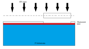
Figure 4: Photolithography
The oxide is etched with hydrofluoric acid where it is not protected by the photo-resist the resultant is shown in Fig.5
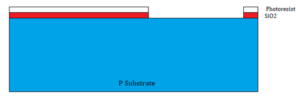
Figure 5: piranha etch
Then the remaining photoresist is stripped away using a mixture of acids called “piranha etch”.
Piranha etch:– Piranha solution also known as a piranha etch is a mixture of sulfuric acid (H2SO4) and hydrogen peroxide (H2O2), used to clean organic residues off substrates.
The well is formed where the substrate is not formed with oxide, there are two ways to add the dopants to create n-well.
1. Diffusion:– In this process, the wafer is placed in the furnace with a gas containing the dopants when heated dopant atoms diffuse into a substrate.
2. Ion Implantation:– In this process dopant ions are accelerated through an electric field and blasted into the substrate.
In either method, the oxide layer prevents the atoms from entering the substrate where no well is intended. Finally, the remaining oxide is stripped off using the Hydrofluoric acid to leave a bare wafer with a well appropriate place, here Ion implantation is used to form an n-well, the resultant is shown in Fig 6 and 7.
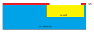
Figure 6: n well formation
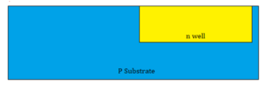
Figure 7: Bare wafer after stripping off the remaining oxide
After formation of n-well gates are formed using the polycrystalline silicon generally called as polysilicon over a thin layer of oxide, polysilicon is better than metal because it does not melt during later process, thin gate oxide is grown in a furnace then the wafer is placed in a reactor with Silane gas (SiH4) and heated again to grow the polysilicon layer through a process called ” chemical vapour deposition”. The polysilicon is heavily doped to form a reasonably good conductor as shown in below Fig 8.
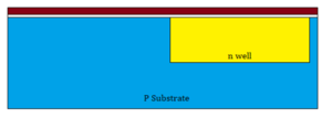
Figure 8: Chemical vapour deposition
Now the wafer is patterned with photoresist and the polysilicon mask leaving the polysilicon gates, the resultant is shown in Fig 9.
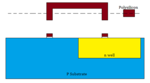
Figure 9: Patterning poly
Now the n+ regions are introduced to the active area and well contact, A protective layer of oxide is formed and patterned with n diffusion mask as shown in Fig 10 and 11.
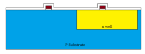
Figure 10: Formation of oxide layer
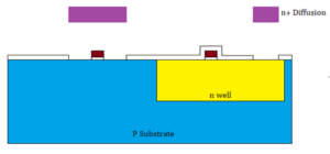
Figure 11: Patterning with n diffusion mask
Formation of n+ diffusion using ion implantation or diffusion. The polysilicon gate over the nMOS transistor blocks the diffusion so that the drain and source are separated by the channel under the gate this is called as self-align process because the drain and source are automatically formed adjacent to the gate without the need of aligning masks then finally the protective layer is stripped off as shown in Fig 12.
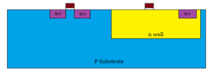
Figure 12: Formation of n+ diffusion
Similarlly the same process is repeated for P+ diffusion to give the structure as shown in Fig 13.
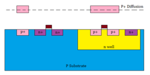
Figure 13: Formation of P+ diffusion
After the formation of the n+ diffusion and the p+ diffusion, a thick field oxide is grown to insulate the wafer from metal and patterned with the contact mask as shown in Fig 14.
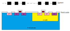
Figure 14: Patterning of contact mask
Finally the Aluminium is sputtered over the entire wafer this process is called as Metalization.
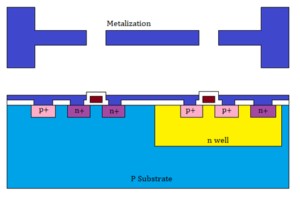
Figure 15: Metalization
Comments are closed.
