Wire Modelling, Cross-talk & Double-switching
Author : Abhishek Kumar, Physical Design Engineer, SignOff Semiconductors
Wire
Wire appears as a simple line in schematic diagrams, connecting two components. But they are equally important as transistors because they affect speed, power dissipation and reliability of the circuit.
Wire Model
Generally we think of wire to be ideal with no resistance, no capacitance, no inductance and an equipotential region . But such a wire is not realizable physically.
Lumped Wire Model
Wires have parasitic capacitance, resistance and inductance distributed along its length.
But it is useful to lump the distributed fractions into a single circuit element when only a single parasitic component is dominant. In the lumped RC model, resistance and capacitance of each wire segment is lumped into single effective resistance R and capacitance C respectively.

Figure 1: Lumped RC
Advantages
- This model is simple and makes the circuit analysis easier as voltage and current can be expressed using ordinary differential equations.
- It gives reasonable approximation of distributed circuit using simple RC network.
Disadvantages
- This model is inaccurate for longer wires.
- The delay calculated using this model is almost double of the actual value.
Distributed Wire Model
This model is used for adequately representing longer interconnect wires. Here the entire resistance and capacitance of wire is distributed along the entire length of the net.

Figure 2: Distributed RC
Advantages
Provides accurate model of behaviour of wire used in the circuit.
Disadvantages
This model is complex and partial differential equations have to be solved for getting voltage values.
Capacitance
Capacitance of a parallel plate capacitor is proportional to the area of overlap between the conductors and inversely proportional to their separation.
Fringing Capacitance
It is the capacitance between the side-walls of the wires and the substrate. Fringing means bending of the electric field lines near the edges of the parallel plate capacitor. In a parallel plate capacitor, electric field lines are parallel to each other. But these field lines do not end abrruptly at the edge and are rather bent at the edges because of non-uniform charge distribution.
Because of this effect, capacitance is more than calculated using the formula for parallel plate capacitance. If the area is doubled, the capacitance will not be double but less than that because fringing effect will not be doubled.
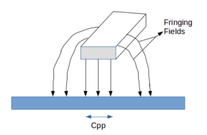
Figure 3: Fringing Capacitance
Coupling Capacitance
Coupling is desirable or undesirable transfer of energy from one conductor to another. When two nets of same metal layer run parallel and close to each other for long distance, the coupling capacitance is very large and it couples significant energy from one net, called an aggressor, to another net, called a victim. This gives rise to cross talk noise and cross talk delay in the circuit.
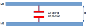
Figure 4: Coupling Capacitance
Cross-talk
It occurs when there are parallel running nets of same metal layer for long distance. When a signal on a net switches very fast then, the wires in its surroundings tends to switch too and their logical values or transition can be affected. This is called cross talk. It causes noise bumps in non-switching nets and advancing/delaying of transition in switching nets.
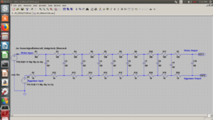
Figure 5: Cross-talk Analysis
Cross-talk Noise
It is undesired change in the logical values of victim due to switching in the input of aggressor. If one net is switching and other is at a constant value , the switching net may cause voltage spikes on other net. This is called as cross talk noise. Cross talk noise is evolving as a key source in degrading performance and reliability of high speed integrated circuits.
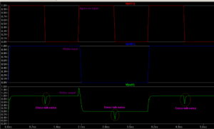
Figure 6: Cross-talk Noise Waveform
Cross-talk Delay
When there is some delay or advancement in output transition of victim due to input transition of aggressor, it is called as cross talk delay. It occurs when some transition is happening in both the nets. Cross talk delay depends on the switching direction of the aggressor and victim nets .
Cross-talk in data path: If aggressor and victim both switch in same direction, victim transition becomes fast resulting data to arrive early, which may cause hold violation. This scenario is good for setup and bad for hold.
Other way, if both switch in opposite direction, victim transition slows down which increases the delay and may result in setup violation. This scenario is bad for setup and good for hold.
Cross-talk in clock path: Cross-talk in clock path is exactly opposite to that in data path. If aggressor and victim both switch in same direction, victim will see improved transition and makes the clock to arrive early which may result in setup violation. This scenario is bad for setup and good for hold.
If both aggressor and victim both switch in opposite direction, clock will arrive late because of bad degraded transition which may lead to hold violation. This scenario is good for setup and bad for hold.

Figure 7: Cross-talk Delay Waveform
How cross-talk effects can be reduced?
- Assign Non default routing (NDR) rules – Increase spacing.
- Insert buffer to split the long nets.
- Jump to different metal layers.
- Shielding – Ground lines run in between the signal lines so that they form coupling capacitance with ground.
- By up-sizing the driver of victim net or downsizing driver of aggressor net.
Double Switching:
When the driver is of lower drive strength and coupling capacitance between adjacent nets is very high, then aggressor transition induces voltage bump in signal present on victim net. If this voltage bump crosses threshold value then the glitch propagates through combinational logic and makes output to switch twice. If this happens in clock net, it can cause double clocking of the flop where the clock switches twice on an active edge or false clocking because of which the voltage bump on the non-sensitive edge can actually capture a data.
As shown below, because of the low drive strength of BUF1, which is the driver of victim net, and the capacitive load of the net, the transition at the input of buffer BUF2 is slow. Because of crosstalk, an aggressor transition causes a voltage bump in signal at the input of buffer BUF2. This causes the output of the buffer to switch twice.
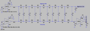
Figure 8: Double-switching analysis
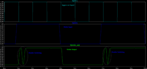
Figure 9: Double-switching waveform
Double switching error: The functional error because of cross-talk effects on victim net which can cause incorrect circuit operation due to glitch propagation through combinational logic, by double clocking on the active edge of a clock signal or by false clocking on non-sensitive edge of clock is known as double switching error.
To fix double-switching violations:
- Decrease the coupling capacitance by
- Increasing the spacing or
- Shielding the adjacent nets.
- Increase the drive strength of victim net driver to reduce the transition time
Comments are closed.
