Synthesis
Author: Batchu Sri Sai Chaitanya, Physical Design Engineer, Signoff Semiconductors
Synthesis is process of converting RTL (Synthesizable Verilog code) to technology specific gate level netlist (includes nets, sequential and combinational cells and their connectivity).
Goals of Synthesis
- To get a gate level netlist
- Inserting clock gates
- Logic optimization
- Inserting DFT logic
- Logic equivalence between RTL and netlist should be maintained
Input files required
- Tech related:
- .tf- technology related information.
- .lib-timing info of standard cell & macros
- Design related:
- .v- RTL code.
- SDC- Timing constraints.
- UPF- power intent of the design.
- Scan config- Scan related info like scan chain length, scan IO, which flops are to be considered in the scan chains.
- For Physical aware:
- RC co-efficient file (tluplus).
- LEF/FRAM- abstract view of the cell.
- Floorplan DEF– locations of IO ports and macros.
Synthesis steps

Fig1: Synthesis Flow
1. Analyze
- Checks syntax on RTL and generates immediate files.
2. Elaborate
- Brings all lower level blocks into synthesis tool.
- All the codes and arithmetic operators are converted into Gtech and DW (Design Ware) components. These are technology independent libraries.
- Gtech- contains basic logic gates &flops.
- DesignWare- contains complex cells like FIFO, counters.
- Elaborate performs following tasks;
- Analyses design hierarchy.
- Removes empty switches and dead branches.
- Executes initial commands.
- Detects asynchronous reset.
- Converts decision trees to mux.
- Converts synchronous to Dlatch/DFF.
- FSM pass
- Detects FSM logic and extracts the no of input, output bits and state bits.
- Converts FSM logic to basic logic.
- Memory pass
- Merging DFF to memory write(memwr) and memory read (memrd)
- Consolidating memwr/memrd cells
- Generate memory (mem) cells
- Mapping mem cells to basic logic
3. Import constraints and UPF
Once the design is extracted in the form of technology independent cells, timing constraints are imported from the SDC file.
If the design consists of multiple power domains, then using the UPF power domains, isolation cells, level shifters, power switches, retention flops are placed.
4. Clock gating
Due to high switching activity of clock a lot of dynamic power is consumed. One of the techniques to lower the dynamic power is clock gating. In load enabled flops, the output of the flops switches only when the enable is on. But clock switches continuously, increasing the dynamic power consumption.
By converting load enable circuits to clock gating circuit dynamic power can be reduced. Normal clock gating circuit consists of an AND gate in the clock path with one input as enable. But when enable becomes one in between positive level of the clock a glitch is obtained.
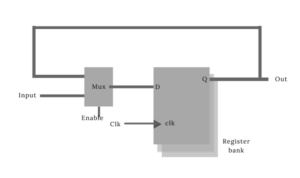
Fig2: Load enabled register bank

Fig3: Clock gated register bank
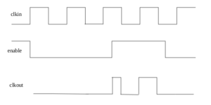
Fig4: Waveform for clock gate
To remove the glitches due to AND gate, integrated clock gate is used. It has a negative triggered latch and an AND gate.
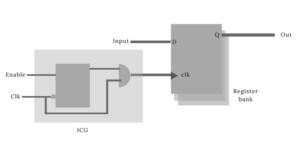
Fig5: Integrated clock gated register bank

Fig6: Waveform for ICG
Clock gating makes design more complex. Timing and CG timing closure becomes complex. Clock gating adds more gates to the design. Hence min bit width (minimum register bit width to be clock gated) should be wisely chosen, because the overall dynamic power consumption may increase.
5. Compile
- Performs Boolean optimization.
- Maps all the cells to technology libraries.
- Performs logic and design optimization.
6. Optimization
- Logic optimization
- Constant folding
- Detect identical cells
- Optimize mux(dead branches in mux)
- consolidate mux and reduce inputs(many to single)
- Remove DFF with constant value
- Reduce word size of the cells
- Remove unused cells and wires
- Design optimization
- Reduce TNS and WNS
- Power Optimization
- Area Optimization
- Meet the timing DRV’s
- incremental clock gating
7. DFT (Design for Testing) insertion
- DFT circuits are used for testing each and every node in the design.
- More the numbers of nodes that can be tested with some targeted pattern, more is the coverage.
- To get more coverage the design needs to be more controllable and observable.
- For the design to be more controllable we need more control points (mux through which alternate path is provided to propagate pattern).
- For the design to be more observable we need more observe point (A scan-able flop that observes the value at that node).
- Scan mode is used to test stuck at faults and manufactured devices for delay.
- Scan mode is done using scan chains
- Scan chains are part of scan based designs to propagate the test data.
- By having scan chains, the design can be more controlable and observable.
- Each scan chain inputs the pattern through scan input and outputs the pattern through scan output.
- Scan chain consists of scan flops where the output of scanflops is directly connected to scan inputs of the flops.
- Stages of scan mode
- Inputs the pattern through scan input port.
- Scan shift- Scan enable is set to 1. Then inputs the pattern through the scan input, shifts the pattern through the scan flops and load all the flops with test pattern.
- Scan capture- Scan enable is set to 0. In one clock cycle the loaded value in the flops propagates through combinational circuit and reaches the D pin of the next flop.
- Scan enable is set to 1 and outputs the pattern through scan output port.
- The scan chain length and number of scan chains has to be properly chosen, as having more scan chain length increases the pattern propagation time and having more scan chains increases the number of scan IO ports.

Fig7: Scan chain
8. Compile incremental
- Technology mapping of DFT circuit
- Optimization of the design
9. Outputs of Synthesis
- netlist
- SDC
- UPF
- ScanDEF- information of scan flops and their connectivity in a scan chain
Checklist
- Check if the RTL and netlist are logically equivalent (LEC/FM).
- Check if SDC and UPF are generated after synthesis and also check their completeness.
- Check if there are any assign statements.
- Checks related to timing
- Combinational loops
- Un-clocked registers
- unconstrained IO’s
- IO delay missing
- Un-expandable clocks
- Master slave separation
- multiple clocks
- Checks related to design
- Floating pins
- multi driven inputs
- un-driven inputs
- un-driven outputs
- normal cells in clock path
- pin direction mismatch
- don’t use cells
Comments are closed.
