What is SDC?
The Synopsys Design Constraints (SDC) format is used to specify the design intent, including timing, power and area constraints for a design. This format is used by different EDA tools to synthesize and analyse a design. SDC is based on the tool command language (Tcl).
SDC file contains the following information:
- SDC version (optional)
- SDC units (optional)
- Design Constraints
- Design Objects
- Comments (optional)
The information specified in design constraints is operating conditions, wire load models, system interface, design rule constraints, timing constraints, timing exceptions, area constraints, multi-voltage & power optimization constraints and logic assignments.
Design constraints will have all the object access commands. Objects can be design, clock, port, pin, cell, net, library, etc.
We will understand the design constraints with reference to the following figure. We will not look at the syntax of SDC commands. The aim of this blog is to understand how SDC file is written for a design.
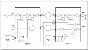
There are two blocks in the design named block A and block B. Two PLLs serve two different clocks to the design. Design constraints will be defined at the I/O pins.
I/O Pins 2, 6, 10 – Clocks are the most important part of a design. As there are two PLLs in the above design, it is clear that there are two different clocks in the design. These clocks must be defined in the timing constraints. At pin IO2 of block A and pin IO6 of block B, the clocks are entering the blocks. Hence are defined using create_clock command at respective pins. This command specifies the period, duty cycle, rise and fall edges of a clock. You can also give name to the clock. Clock CK1 is also going to the clock pins of flops in block 2. So, we have to define clock CK1 at IO10 of block 2 also.
e.g. create_clock -period 10 -waveform {0 6} -name my_clk1 [get_ports IO2]
I/O Pin 1 – Input port is applied with the command set_driving_cell. Doing this causes the port to have a cell delay that is load-dependent value of external cell which is driving that port. In the design shown in the figure, buffer is an external cell which is driving the input port of block A. Doing this helps us to have accurate external delay which is required for timing calculations.
e.g. set_driving_cell -lib_cell BUF [get_ports IO1]
Clock generators 3, 7 – There can be a number of clock generator circuits in the given design. Frequency of these generated clocks is different than the master clock. Clock generators can be used for multiplying, dividing or just inverting the master clock to derive a new generated clock. As frequency is changing, we have to define them as new generated clocks at the output of clock generator circuit. create_generated_clock command is used for this purpose. While defining generated clocks, we must specify the master clock.
e.g. create_generated_clock -divide_by 2 -source [get_ports IO2] -name clk_div [get_registers FF2]
I/O Pin 4 – To do constraint checking at the output port, set_output_delay command is used. This command calculates the delay between output port and the next sequential cell (which captures data from this output port.) But when we think about block level design, we will not be knowing that where the output port is connected. Still we should calculate the output delay. To favor this, virtual clock is defined. This virtual clock is same as the normal clock but it does not have any real existence.
e.g. set_output_delay 1.7 -clock my_clk1 [all_outputs]
I/O Pin 5 – Similar to output delay, input delay is calculated. set_input_delay command is used to calculate the timing requirements at the input port. It will calculate timing of the external path to the input port.
I/O Pin 11 – set_load command is used to describe an external load capacitance connected to the top level port. This command considers pin as well as wire capacitance. This command helps us to time the design accurately.
e.g. set_load 20 [get_ports IO11]
As there are two different clocks (i.e. asynchronous clocks) in the design, any path which starts from CK1 and goes to CK2 should not be considered for timing analysis. Best way to achieve this is setting these clock as asynchronous. set_clock_group command specifies whether clock groups are synchronous, asynchronous or exclusive.
In this example, CK1 and CK2 are set as asynchronous clocks. In block 2, the output of mux is going to FF5. Input to the mux are CK2 and a generated clock with CK2 as a master clock. But at a particular instance of time, only one clock will go to the output of a mux. Hence, these two clocks are set as mutually exclusive clocks.
Timing Exceptions:
1. Falsepath:
Some paths in the design need not to be considered for the timing analysis. There can be multiple reasons to set a path as a falsepath. One of the reasons is shown in the above design. CK1 and CK2 are asynchronous clocks, so we set any path from CK1 to CK2 as a falsepath. set_false_path command is used for this purpose. Path from FF4 to FF5 is a false path because both the flops are driven by different clocks.
e.g. set_false_path -from [get_clocks my_clk1] -to [get_clocks my_clk2]
2. Max & Min path:
I/O Pins 8, 9 – The path groups are of four types: input-to-reg, reg-to-output, reg-to-reg and input-to-output. The path from input pin IO8 to output pin IO9 of block A is input-to-output. In such cases, we have to constrain these paths to maximum delay or minimum delay. set_max_delay and set_min_delay commands are used to define these delays.
e.g. set_max_delay 0.15 -from IO8 -to IO9
3. Multi-cycle path:
Data takes one clock cycle to propagate from launch flop to capture flop. But it can also take more than one clock cycle. We should set such paths to multi-cycle path using set_multicycle_path command. Multi-cycle path is always a multiple of the clock cycle.
Comments are closed.
