Author – Challa Krishnachaitanya Reddy With 20+ years in Design has worked on tapeouts at sub-5nm
VLSI Design at 2nm and Below: Navigating Nanosheet Complexity with AI
The VLSI industry is no longer just scaling transistors – it is navigating a fundamental shift in how design complexity behaves.
At older nodes, improvements were largely linear. Shrink the geometry, optimize timing, fix power, and iterate. Engineers could rely on experience-driven heuristics, and tools from companies like Synopsys, Cadence Design Systems, and Siemens EDA handled most of the heavy lifting with predictable convergence.
At 2nm and below, this predictability breaks.
We are moving into an era where:
-
- Device architecture (FinFET → GAA nanosheets)
-
- Power delivery (frontside → backside)
-
- Routing constraints
-
- Variability and coupling effects
…are no longer independent variables.
They are deeply interdependent systems.
This creates a new class of challenge:
Not scaling, but managing interactions across the entire design space
And that is where the narrative of this article begins.
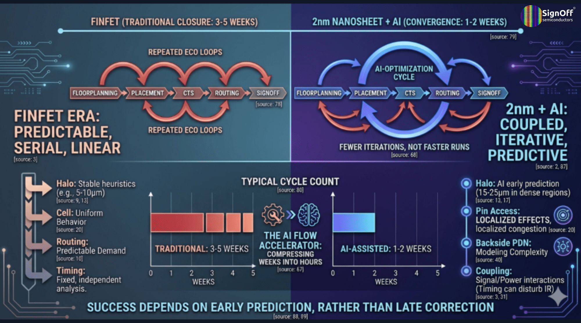
From Predictable Flows to Coupled Systems
In FinFET-based designs, closure was largely sequential:
-
- Fix timing → then fix IR → then clean routing
At nanosheet nodes, this sequence collapses into a loop:
-
- Fixing timing disturbs IR
-
- Fixing IR increases congestion
-
- Fixing congestion impacts CTS
Closure becomes iterative and cyclic, not linear.
This is the core complexity shift-and it reflects across every stage of physical design.
Floorplanning: When Heuristics Stop Working
FinFET floorplanning relied heavily on past design patterns. Macro halos, spacing, and routing expectations were stable.
At nanosheet nodes:
-
- Routing demand becomes less predictable
-
- Pin accessibility varies significantly
-
- Congestion spreads beyond macro boundaries
Real-world impact:
-
- Halo sizes grow from ~5-10µm to ~15-25µm
-
- Clean early floorplans fail post-CTS
-
- Late macro movement adds 2-4 days of rework
AI tools like DSO.ai and Cerebrus don’t “solve” floorplanning—they reduce the probability of bad early decisions.
Placement: Local Effects Become Global Problems
In FinFET:
-
- Cells behaved uniformly
-
- Placement quality was stable
In nanosheet:
-
- Cell behavior varies with nanosheet configuration
-
- Pin access introduces localized congestion patterns
Observed challenges:
-
- Timing-clean placement failing after routing
-
- IR hotspots forcing late-stage spreading
-
- Extra placement-to-route loops (0.5-1 day each)
AI-assisted placement helps avoid known failure patterns, improving first-pass quality rather than eliminating iterations.
CTS: The Hidden Coupling Problem
Clock Tree Synthesis becomes more sensitive due to:
-
- Backside power delivery
-
- Increased coupling with signal and power nets
Real observations:
-
- Post-route skew shifts of 20–50ps
-
- Unpredictable shielding behavior
-
- 2-3 ECO cycles for skew closure
AI helps flag high-risk regions early—but final closure still depends on extraction accuracy and engineering judgment.
Power Planning: Freedom with Complexity
Backside power delivery is a breakthrough—but it introduces:
-
- Alignment issues visible only after extraction
-
- Complex EM behavior due to split current paths
-
- Interaction between frontside and backside networks
Typical impact:
-
- 2-4 IR/EM ECO loops
-
- Each loop costing half a day or more
AI shifts the approach from brute-force analysis to risk-driven prioritization.
Routing: Decisions That Cannot Be Undone
Routing at 2nm is constrained by:
-
- Limited usable layers
-
- Interaction with clock and power structures
Key observations:
-
- Early layer assignment becomes critical
-
- Congestion appears late (post-detailed routing)
-
- 2-3 routing iterations, each taking 6 -12 hours
AI doesn’t make routing faster—it makes fewer full re-routes necessary.
Signoff: Dual-Domain Complexity
Signoff now spans:
-
- Frontside + backside interactions
-
- Increased DRC/LVS complexity
-
- Timing correlation gaps
Tools like Calibre, IC Validator, and Pegasus remain essential, but:
-
- Debug volume increases significantly
-
- Only a fraction of violations are truly critical
AI helps in classification and prioritization, saving 1-2 days of debug effort.
The Real Role of AI: Reducing Iterations, Not Runtime
A key misconception is that AI speeds up tools.
It doesn’t.
What it does:
-
- Reduces unnecessary iterations
-
- Improves alignment across stages
-
- Increases first-pass success probability
In practice:
-
- Traditional closure: 3–5 weeks
-
- AI-assisted closure: 1–2 weeks
-
- Stage runtimes remain similar—but iteration count drops significantly
Reality Check: AI Is Powerful, Not Magical
AI effectiveness depends on:
-
- Cost function definition
-
- Training data quality
-
- Engineer guidance
Poor setup can lead to misleading optimizations.
Which leads to an important takeaway:
-
- AI does not replace engineers
It amplifies good engineering decisions
- AI does not replace engineers
Conclusion: The Shift Is Philosophical
FinFET design lived in a world of predictability and sequential fixes.
Nanosheet design operates in a world of:
-
- Coupled systems
-
- Iterative convergence
-
- Multi-domain interactions
-
- Success at advanced nodes depends on:
Early prediction instead of late correction
- Success at advanced nodes depends on:
AI is not just an optimization tool anymore—it is becoming a navigation system for design complexity.
And in this new landscape, the winning teams are not the ones with better tools…
…but the ones making better decisions earlier in the flow.
Ready to simplify your 2nm design complexity?
Connect with our Signoff Semiconductors VLSI experts to explore AI-driven P&R strategies that improve first-pass success and reduce costly iterations.
Want to dive deeper into this topic? Talk to our experts and explore tailored solutions
Comments are closed.