Author – Challa Krishnachaitanya Reddy With 20+ years in Design has worked on tapeouts at sub-5nm
Why LVS Debugging Breaks at 2nm: The Hidden Complexity of GAAFET Verification
Abstract
As semiconductor technology advances toward the 2nm node, traditional Layout Versus Schematic (LVS) debugging methodologies are becoming increasingly inadequate. The transition from FinFET to Gate-All-Around (GAAFET) architectures introduces vertically stacked nanosheet devices, backside power delivery, and complex interconnect topologies. These changes transform LVS from a deterministic connectivity verification task into an interpretation-driven problem dependent on extraction accuracy and modeling fidelity. This paper analyzes key LVS failure mechanisms observed in advanced node designs and outlines practical strategies to improve verification convergence.
Index Terms
GAAFET, LVS, 2nm, Physical Design, Backside Power Delivery, Nanosheet, Verification, Semiconductor
I. Introduction
Layout Versus Schematic verification has historically been one of the most stable and predictable stages in the physical design flow. At mature nodes, LVS debugging was largely deterministic due to well-defined device architectures and planar connectivity assumptions. Typical issues such as missing pins, incorrect net labeling, or connectivity mismatches could be identified and resolved efficiently through iterative debugging.
However, as the semiconductor industry transitions to the 2nm node, this predictability is diminishing. The introduction of GAAFET architectures fundamentally alters device geometry, connectivity representation, and power delivery mechanisms. Consequently, LVS verification must now account for three-dimensional device structures and multi-domain interactions, making traditional debugging approaches insufficient.
II. Evolution of LVS Problem Space
In FinFET-based designs, LVS engines primarily verified planar connectivity between devices and interconnects. The abstraction between layout and schematic was relatively direct, allowing for deterministic extraction and comparison.
In contrast, GAAFET designs introduce vertically stacked nanosheets forming the channel region, along with backside power delivery networks that decouple power routing from signal layers. These advancements require LVS tools to interpret complex three-dimensional device intent from two-dimensional layout representations. As a result, LVS failures are increasingly caused by discrepancies in interpretation between layout, extraction models, and rule decks rather than explicit physical errors .
III. Key LVS Failure Mechanisms in GAAFET Designs
A. Nanosheet Connectivity Interpretation
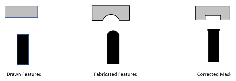
One of the primary challenges in GAAFET-based LVS arises from incorrect interpretation of nanosheet stacking. Vertically aligned nanosheets that are physically connected may be extracted as independent devices due to insufficient modeling of stacking relationships. This results in false open-circuit errors during LVS comparison. Addressing this issue requires pre-LVS nanosheet verification and explicit definition of connectivity within rule decks to ensure correct extraction behavior .
B. Backside Power DeliveryModeling
Backside power delivery introduces a paradigm shift in power network representation. Unlike traditional designs where power is routed through frontside metal layers, advanced nodes utilize backside routing to improve performance and routing efficiency. LVS tools that are not configured to recognize backside connectivity may incorrectly report power nets as floating. Accurate LVS results therefore depend on enabling backside-aware extraction and incorporating appropriate technology files prior to verification .
C. Forksheet-Induced Device Interaction
Emerging forksheet architectures reduce spacing between adjacent devices to achieve higher density. However, this introduces risks of unintended electrical interactions, such as gate-to-source or gate-to-drain shorts. These effects are often influenced by lithographic constraints and are not always captured by conventional spacing rules. Enhanced verification strategies incorporating process-aware checks are required to detect and mitigate such issues .
D. Via Pillar Extraction Discrepancies
At advanced nodes, interconnect structures frequently employ vertically stacked via pillars rather than single vias. LVS extraction engines may misinterpret these structures, representing multiple vias as a single connection. This leads to mismatches between layout and schematic representations. Accurate modeling of via pillars, including verification of via count and structure, is essential to resolve these discrepancies .
E. RibbonFETSource and Drain Modeling
RibbonFET architectures extend nanosheet structures to form source and drain regions. Inadequate recognition of these extensions during extraction can result in false open-circuit violations. Specialized extraction rules and validation checks are necessary to ensure correct interpretation of these device features .
F. Density-Driven Verification Constraints
Nanosheet density plays a critical role in manufacturability and device performance. Violations of density constraints can lead to inconsistencies in both design rule checking and LVS verification. Maintaining density within acceptable limits and incorporating density validation into preprocessing steps are therefore essential for reliable verification outcomes .
IV. Pre-LVS Verification Methodology
To address the increasing complexity of LVS debugging, modern design flows incorporate pre-LVS validation techniques aimed at identifying major issues prior to full verification. These techniques include nanosheet connectivity checks, backside power validation, and preliminary LVS dry runs. Such preprocessing steps, typically executed within minutes, significantly reduce the number of iterations required for final LVS closure and improve overall design efficiency.
V. System-Level Nature of LVS at Advanced Nodes
At the 2nm node, LVS verification must be viewed as a system-level problem involving multiple interdependent components. Accurate results depend on the alignment between rule decks, extraction models, layout intent, and process assumptions. Any inconsistency among these elements can lead to incorrect LVS outcomes, highlighting the need for holistic verification strategies that extend beyond traditional tool-centric approaches.
VI. Observations from Advanced NodeTapeouts
Empirical observations from advanced node tapeouts indicate that traditional LVS methodologies result in high initial failure rates due to inadequate modeling of GAAFET-specific features. However, the adoption of advanced verification techniques, including dual-deck extraction and backside-aware modeling, has led to substantial improvements. Reports suggest that first-pass LVS success rates can approach approximately ninety-six percent when these methodologies are applied effectively .
VII. Conclusion
The transition to GAAFET architectures at the 2nm node represents a fundamental shift in LVS verification methodology. Traditional approaches based on planar connectivity assumptions are no longer sufficient to address the complexities introduced by three-dimensional device structures and advanced power delivery mechanisms.
Future LVS methodologies must emphasize accurate modeling, early validation, and cross-domain integration to ensure reliable verification outcomes. Ultimately, successful LVS closure at advanced nodes requires a shift in engineering perspective from reactive debugging to proactive interpretation and validation of design intent.
Comments are closed.