Author – Challa Krishnachaitanya Reddy With 20+ years in Design has worked on tapeouts at sub-5nm
How to Close Timing at 7nm: 5 Lessons Every Physical Design Team Should Know Why Timing Closure at 7nm Is Different
As semiconductor designs move to advanced process nodes, timing closure becomes significantly more challenging. At 7nm, traditional optimization techniques often fall short due to increased process variations, complex routing congestion, tighter design margins, and growing interactions between timing, power, and signal integrity.
What makes timing closure particularly challenging at 7nm is the transition from single-scenario optimization to Multi-Corner Multi-Mode (MCMM) convergence. A design that meets timing requirements in one process, voltage, and temperature condition may fail in another. As a result, successful timing closure requires simultaneous convergence across functional, test, process, voltage, and temperature scenarios rather than focusing solely on setup and hold closure in isolation.
Based on our experience supporting advanced-node tapeouts, here are five critical lessons that can help engineering teams successfully close timing at 7nm.

Lesson 1: Start Signoff Analysis Early
One of the most common mistakes in advanced-node projects is treating signoff timing analysis as a final checkpoint.
At 7nm, timing issues discovered late in the implementation cycle can trigger costly iterations that affect schedule, power, and area targets. Early signoff-driven analysis helps identify potential bottlenecks before they become critical.
In an MCMM environment, timing fixes are rarely localized. A setup fix applied in one corner may create hold violations in another mode, while a hold fix may degrade setup margin elsewhere. Early signoff visibility enables teams to identify and resolve these interactions before they become ECO-intensive problems.
- Run signoff-quality STA throughout implementation.
- Validate timing with realistic parasitic estimates.
- Track timing convergence across all design milestones.
- Correlate implementation and signoff tools continuously.
- Monitor timing convergence across all active modes and corners rather than relying solely on worst-path reporting.
Early visibility enables teams to address timing challenges proactively rather than reactively.
Lesson 2: Prioritize Clock Network Quality
The clock tree remains one of the largest contributors to timing uncertainty at advanced nodes.
At 7nm, clock skew, jitter, on-chip variation, and routing congestion can significantly impact timing margins. A poorly optimized clock network often becomes the root cause of persistent setup and hold violations.
- Clock architecture planning
- Useful skew optimization
- Clock latency balancing
- Clock shielding and routing strategies
- Variation-aware clock analysis
- Clock-gating timing closure
- Cross-corner clock behavior validation
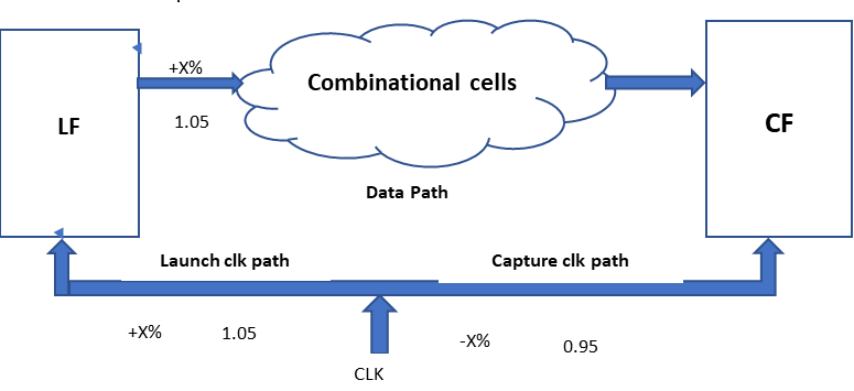
Advanced clock signoff methodologies also leverage Common Path Pessimism Removal (CPPR) to eliminate unnecessary pessimism introduced during timing analysis. Combined with useful skew optimization and variation-aware clock modeling, CPPR helps improve timing correlation, provides a more realistic view of clock path behavior, and reduces the likelihood of over-fixing violations during implementation and signoff.
Investing effort in clock network optimization early can dramatically improve overall timing closure success.
Lesson 3: Manage Variation Aggressively
- Advanced On-Chip Variation (AOCV)
- Parametric On-Chip Variation (POCV)
- Voltage fluctuations
- Temperature variations
- Manufacturing process uncertainties
Ignoring variation until the final signoff stage often results in unexpected violations and missed tapeout schedules.
Recommended Approach
Adopt variation-aware optimization throughout the implementation flow and continuously validate timing across all corners and modes.
At advanced nodes, variation-aware timing analysis and MCMM closure are tightly coupled. Paths that appear clean under nominal conditions frequently become critical when realistic process, voltage, and temperature variation models are applied.
POCV-based signoff methodologies provide a more realistic representation of silicon behavior and help reduce late-stage timing surprises.
Design teams should ensure that variation-aware optimization is performed consistently throughout implementation rather than being deferred to final signoff.
Lesson 4: Address Routing Congestion Before It Impacts Timing
- Longer routing paths
- Increased coupling capacitance
- Higher RC delays
- Signal integrity concerns
- Increased timing uncertainty
- Perform early congestion analysis.
- Optimize floorplan utilization.
- Improve macro placement.
- Use congestion-driven placement techniques.
- Monitor critical path routing continuously.
Because congestion-driven effects often vary across corners, routing-related degradation commonly manifests as MCMM timing failures late in the implementation cycle.
Design teams that solve congestion early often experience faster timing convergence and fewer ECO cycles.
Lesson 5: Optimize Timing, Power, and Signal Integrity Together
- Timing
- Power Integrity
- Electromigration
- IR Drop
- Crosstalk
- Noise Effects
A Signoff-Centric Methodology
- Static Timing Analysis (STA)
- Signal Integrity Analysis
- Power Integrity Verification
- Physical Verification
- Reliability Checks
Voltage-aware timing analysis has become increasingly important at advanced nodes. Localized IR drop can alter cell delays, shift clock arrival times, and create timing failures in corners that previously appeared clean.
Coupling-induced delay shifts can significantly impact setup and hold margins and must be considered throughout implementation.
A unified signoff strategy helps avoid unnecessary ECO iterations and improves overall design quality.
The Growing Importance of Signoff Expertise at 7nm
The challenge is no longer achieving positive slack in a single operating condition.
Modern signoff success depends on achieving simultaneous convergence across timing, signal integrity, power integrity, reliability, and physical verification requirements under all signoff scenarios.
Teams that rely solely on implementation-stage optimization often encounter schedule risks and multiple tapeout delays.
Partnering with experienced signoff engineers can accelerate timing convergence, improve correlation, and reduce project risk across advanced technology nodes.
At Signoff Semiconductors, we help design teams achieve robust timing closure through comprehensive signoff methodologies, advanced STA expertise, and proven experience across 7nm and below process technologies.
Final Thoughts
Timing closure at 7nm requires more than aggressive optimization. Timing closure at 7nm is fundamentally an MCMM convergence challenge rather than a simple setup-versus-hold optimization exercise.
Every timing fix must be evaluated across multiple process, voltage, temperature, functional, and test scenarios while maintaining correlation between timing, power, signal integrity, and reliability signoff requirements.
It demands a signoff-first mindset that incorporates variation awareness, clock quality, congestion management, and cross-domain verification throughout the design cycle.
By combining MCMM-aware optimization, variation-aware analysis, extraction correlation, power-integrity-aware timing, and crosstalk-aware verification, engineering teams can significantly improve timing convergence, reduce ECO effort, and achieve faster, more predictable tapeout success.
Comments are closed.