Author – Saraswati Bhat, Software Engineer – I – Embedded
Embedded SoC Design Mistakes Startups Must Avoid
The race to build innovative semiconductor products is accelerating as startups enter markets such as Artificial Intelligence (AI), Internet of Things (IoT), automotive electronics, consumer devices, industrial automation, and edge computing. While the opportunity is enormous, designing a successful System-on-Chip (SoC) remains one of the most complex engineering challenges in the semiconductor industry.
Many startups focus heavily on product features and time-to-market but often underestimate the technical and business risks associated with SoC design and development. A single design mistake can result in costly re-spins, delayed product launches, increased verification cycles, and significant budget overruns.
At SignOff Semiconductors, we have worked with global semiconductor companies and startups across the ASIC and SoC development lifecycle. Based on our experience, here are some of the most common Embedded SoC design mistakes startups must avoid.
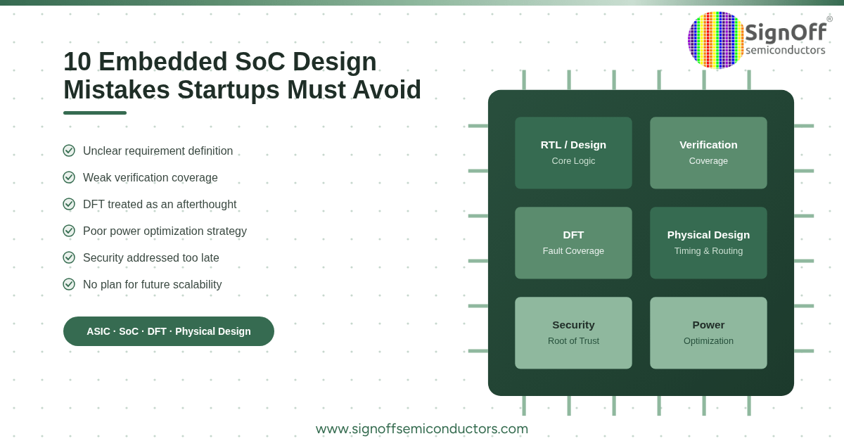
Inadequate Requirement Definition
One of the biggest reasons SoC projects fail is unclear or incomplete specifications at the beginning of the design cycle.
Many startups rush into architecture design without fully understanding:
- Functional requirements
- Performance targets
- Power consumption goals
- Security requirements
- Scalability needs
- Cost constraints
A poorly defined specification often leads to multiple design revisions later in the project.
Best Practice
Invest sufficient time in system-level planning and requirement analysis before starting RTL design. A clear product roadmap helps prevent expensive changes during later stages of development.
Underestimating Verification Complexity
Industry studies consistently show that verification consumes a significant portion of the semiconductor design cycle. Yet many startups allocate most resources to design and far less to verification.
A chip may appear functionally correct during development but still fail in real-world applications due to hidden bugs.
Common verification gaps include:
- Insufficient test coverage
- Limited corner-case testing
- Inadequate protocol validation
- Poor regression strategies
Best Practice
Adopt a robust verification methodology early. Comprehensive verification planning reduces silicon failures and improves first-pass silicon success rates.
Ignoring Design-for-Test (DFT) Requirements
Many startups view Design for Testability (DFT) as a secondary activity that can be addressed later in the project.
This approach often creates challenges during manufacturing and post-silicon validation.
Without proper DFT implementation, organizations may struggle with:
- Low fault coverage
- Reduced manufacturing yield
- Increased debugging complexity
- Higher production costs
Best Practice
Integrate DFT planning during the architecture and RTL stages rather than treating it as a final step.
Poor Power Optimization Strategy
Modern semiconductor products must balance performance and energy efficiency.
Startups frequently focus on achieving maximum performance without considering power consumption, especially in applications such as:
- IoT devices
- Wearables
- Automotive electronics
- Edge AI systems
- Battery-powered products
Excessive power consumption can shorten battery life, increase thermal issues, and limit product adoption.
Best Practice
Incorporate power-aware design techniques from the beginning, including clock gating, power gating, voltage optimization, and low-power verification methodologies.
Choosing the Wrong IP Integration Strategy
Third-party Intellectual Property (IP) blocks help accelerate SoC development, but improper integration can create significant challenges.
Common issues include:
- Interface mismatches
- Performance bottlenecks
- Security vulnerabilities
- Verification complexities
- Licensing complications
Best Practice
Carefully evaluate IP vendors, compatibility requirements, and long-term support before integration.
Neglecting Security in SoC Design
As connected devices continue to grow, hardware-level security has become a critical requirement.
Many startups prioritize functionality and overlook security until late in development.
Potential risks include:
- Data breaches
- Firmware attacks
- Unauthorized access
- Intellectual property theft
Best Practice
Implement security architecture early through secure boot mechanisms, hardware root of trust, encryption engines, and secure communication protocols.
Failing to Planfor Scalability
Startups often design SoCs around immediate product requirements without considering future versions.
As markets evolve, additional features may require:
- More processing capability
- Enhanced connectivity
- AI acceleration
- Expanded memory support
A rigid architecture can make future upgrades difficult and expensive.
Best Practice
Develop scalable architectures that support future product generations while minimizing redesign efforts.
Insufficient Physical Design Planning
Even a functionally correct design can encounter problems during implementation if physical design considerations are ignored.
Common challenges include:
- Timing violations
- Signal integrity issues
- Routing congestion
- Thermal limitations
- Area inefficiencies
Best Practice
Physical design teams should be involved early to ensure architecture decisions align with implementation realities.
Unrealistic Development Timelines
Many startups operate under intense market pressure and set aggressive schedules.
While speed is important, compressed timelines often result in:
- Reduced verification coverage
- Increased design errors
- Missed quality targets
- Higher re-spin risks
Best Practice
Build realistic project plans that account for design, verification, DFT, physical implementation, and post-silicon validation.
Not Partnering with Experienced Semiconductor Experts
Building an SoC requires expertise across multiple domains, including:
- ASIC Design
- RTL Development
- Functional Verification
- Physical Design
- DFT Engineering
- Embedded Software
- Post-Silicon Validation
Many startups lack specialized resources in all these areas.
Best Practice
Partnering with experienced semiconductor engineering companies can significantly reduce risk, accelerate development, and improve silicon success rates.
How SignOff Semiconductors Helps Startups Succeed
At SignOff Semiconductors, we provide end-to-end semiconductor engineering services that help startups transform innovative ideas into production-ready silicon.
Our expertise includes:
- ASIC Design and Development
- SoC Architecture Design
- Functional Verification
- Physical Design
- DFT Solutions
- Embedded Systems Engineering
- FPGA Development
- Semiconductor Product Engineering
By combining deep technical expertise with proven industry methodologies, we help startups reduce design risks, shorten development cycles, and achieve faster time-to-market.
Conclusion
Developing a successful Embedded SoC requires more than innovative ideas. It demands careful planning, robust verification, effective DFT implementation, power optimization, security integration, and scalable architecture decisions.
Avoiding these common SoC design mistakes can significantly improve product quality, reduce development costs, and increase the likelihood of first-pass silicon success.
As semiconductor technologies continue to evolve, startups that adopt best practices and leverage experienced engineering partners will be better positioned to compete in today’s fast-moving electronics and semiconductor landscape.
Comments are closed.