By – SignOff Semiconductors
Are We Ready to Tape Out?” Notes From the Meeting Every ASIC Team Has
There is a meeting that happens on every ASIC programme. Nobody puts it on the calendar with that name, but everyone knows when it has arrived.
The tapeout date is a few weeks out. The foundry slot is booked. Someone senior, maybe the programme manager, maybe a founder who has investors asking, looks around the room and asks the question everyone has been quietly avoiding: are we actually ready?
The room goes a bit quiet.
We have sat in a lot of these meetings, on our own programmes and on customers’ programmes. And the honest answer is almost never a clean yes. It is usually “yes, but…” followed by a list of small things that nobody quite owns. None of them is a disaster on its own. Together, they are why engineering leads don’t sleep well in the month before tapeout.
Here are the things we see on that list most often, and what we have learned about keeping them off it.
“We both read the spec. We just read it differently.”
A surprising number of silicon bugs are not really bugs. They are two smart engineers who each built exactly what the specification said, as they understood it.
The RTL designer reads a line about reset behaviour one way. The verification engineer reads it another way, and writes tests that pass against the first interpretation. Everything looks green. The difference only shows up on the bench, in one operating mode, months later.
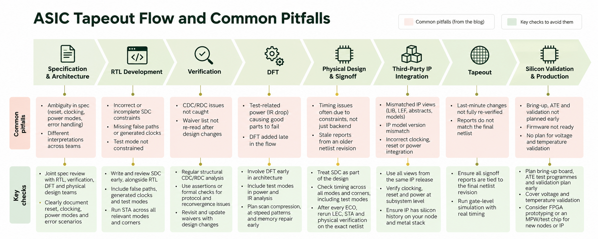
The fix is boring and it works: get the RTL, verification, DFT and physical design people into the spec review, not just the architects. Ambiguity tends to hide in the same few places every time: reset, clocking, power modes and what happens when something goes wrong. If those are written down explicitly, a lot of late-night debug simply never happens.
“Timing is the problem.” (It usually isn’t.)
When a team is fighting timing in the last month, the instinct is to blame the backend. More often than not, what they are really fighting is a constraint problem that was written months earlier, or not written at all until synthesis forced the issue.
A missing false path creates violations that aren’t real, and physical design burns days chasing them. An over-broad false path or a wrongly defined generated clock does the opposite: it hides violations that are real. A test mode nobody constrained can do either. We have come to think of SDC constraints as part of the design, written alongside the RTL and checked with tools, not something handed over at netlist time. And timing should be looked at across every mode and corner that matters, test modes included, with proper on-chip-variation derates. It is far cheaper than discovering a corner nobody ran.
The waiver list nobody has re-read
Every programme has one. A list of CDC and RDC waivers, each marked “reviewed, safe,” some of them from a version of the design that no longer exists.
Clock-domain crossing bugs are some of the nastiest to find in silicon. They are intermittent, and RTL simulation does not model metastability, so they can pass every test you have. Structural CDC analysis catches missing or wrong synchronisers; protocol and reconvergence issues usually need assertions or formal checks on top. Both only help if they are run regularly, not just before signoff, and if someone actually re-reads the waivers when the design changes. In our experience, that list is where yesterday’s “known safe” quietly becomes today’s risk.
The chip that simulated perfectly and still didn’t wake up
Most SoCs today have several power domains, and power intent is one of the easiest things to get subtly wrong. A missing isolation cell, a level shifter in the wrong place, a retention register that doesn’t actually retain. The functional simulation can be flawless and the chip can still fail to come out of sleep.
The usual cause is mundane. The UPF file drifted out of step with the RTL somewhere along the way. Keeping power intent under the same version control as the RTL, running power-aware simulation, and re-checking it after synthesis and after place-and-route, when cells get inserted and moved, catches most of this before it costs a respin.
Good parts failing on the tester
This one surprises people who haven’t seen it before. The design is correct. Functional IR drop is fine. Then the parts go on the tester and a worrying number fail.
The reason is that scan shift and at-speed capture can switch far more of the chip at once than normal operation ever does. That extra current can cause IR drop that functional analysis never looked at, and good silicon fails for the wrong reasons. It is why we like DFT in the room from architecture, not bolted on after synthesis, and why test modes belong in power and IR analysis alongside functional ones. Scan compression, at-speed patterns and memory repair all go more smoothly when they are planned early, too.
“The IP vendor sent an update last week”
Third-party IP saves months: processor cores, memories, SerDes, PHYs. But in our experience, IP problems rarely come from the IP itself. They come from assumptions at the boundary.
The timing view and the physical view don’t quite match. The simulation model is one release behind. A hard macro is hooked up to the wrong power rail. It’s worth checking that every view (LIB, LEF, abstracts, models) comes from the same release, that the IP has real silicon history on your node and metal stack, and that someone has verified the macro’s clocking, reset and power at subsystem level, not just at the top.
“That report is from Tuesday’s netlist”
This is the one that makes signoff leads wince. The timing report looks clean. So does LVS. Then someone notices the reports were generated before the last ECO.
Late changes are a fact of life. A bug turns up in the final regression, a timing path needs one more fix, and the change has to go in. The risk isn’t the change. It’s what doesn’t get re-run afterwards. After every ECO, functional or timing, equivalence checking (LEC), the affected regressions, STA and physical verification need to run again on the exact database going to the foundry. Gate-level simulation with real timing is worth running too, because it catches reset, X-propagation and scan-mode issues that RTL simulation often misses.
It sounds obvious written down. At 11pm, three days before tapeout, it is very easy to skip. That’s why we like every signoff report tied to a specific netlist revision, so a stale one is impossible to miss.
One more thing worth doing early: leave spare cells and some room in the floorplan. If a bug does turn up in silicon, it can then often be fixed with a metal-only ECO, changing a few masks instead of the full set. That is still painful, but it is a lot less painful than a full respin.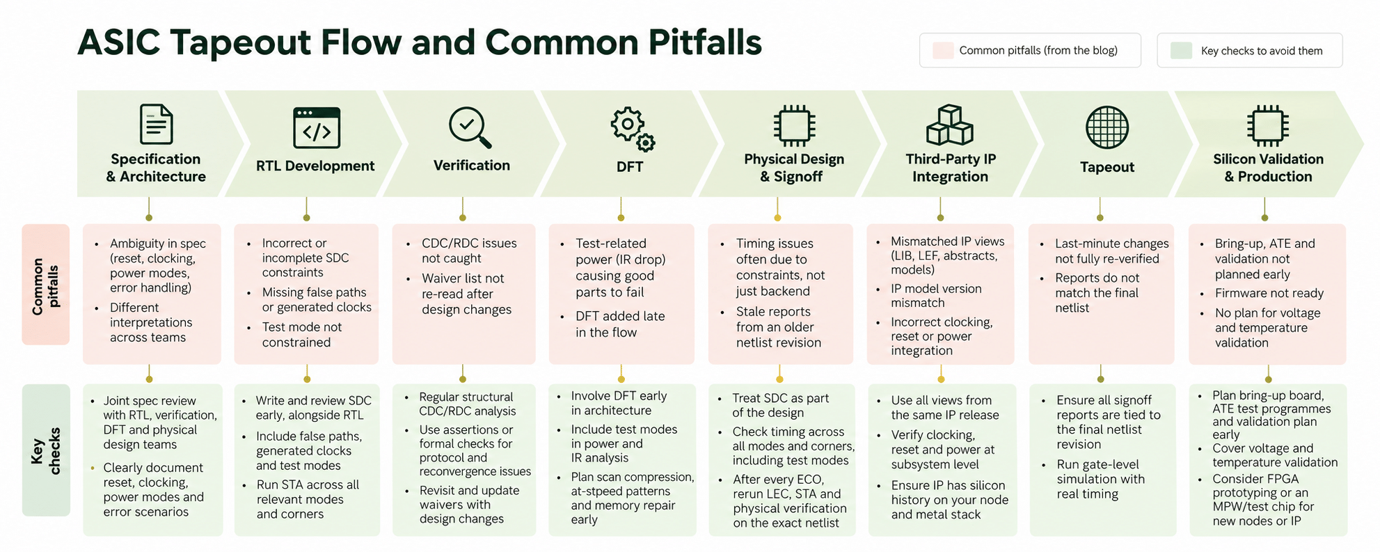
Forgetting that tapeout isn’t the finish line
The GDS goes to the foundry, there is a small celebration, and everyone exhales. Then the silicon comes back in a few months, and the questions start. Who has the bring-up board? Are the ATE test programmes ready? Who owns debug if something is off?
The smoothest bring-ups we have seen were planned while the design was still being built: FPGA prototyping so firmware was ready before silicon, test programmes written before tapeout, a validation plan that covered voltage and temperature, not just room-temperature basics. And for a new node, a new analog block or an unproven IP, an MPW shuttle or a small test chip first can save a great deal of pain later.
What all of these have in common
Look back at that list and something stands out. Almost none of these problems are hard because the engineering is unknown. Every team knows CDC matters, that UPF needs checking, that reports should match the netlist.
They happen because the work passes between people. The spec goes to RTL, RTL to verification, the netlist to physical design, the patterns to the tester, the GDS to the foundry, the die to the package house. Every handoff is a small chance for an assumption to change without anyone noticing.
When those stages are spread across several vendors, the gaps get wider. Each one signs off its own piece, and the risk that sits between the pieces belongs to nobody.
That is a big part of why many teams, especially those building their first or second chip, choose one partner to own the programme from specification to silicon. Not because any single stage is magic, but because one team, one set of baselines and one risk register means fewer gaps for things to fall through.
Where we come in
At SignOff Semiconductors, that end-to-end ownership is what our turnkey ASIC work is built around: from architecture and RTL through verification, DFT, physical design and signoff, to tapeout, foundry and OSAT coordination, and silicon validation. Our teams bring the experience of more than 100 tapeouts between them, with physical design work on processes from 180nm to TSMC 5nm. For teams that want to keep some stages in-house, we also work as an ODC, on a build-operate-transfer basis, or as added engineering capacity.
If you have a tapeout coming up and that readiness meeting is already on your mind, we are always glad to talk it through.
Let’s talk: sales@signoffsemi.com
Comments are closed.