By – SignOff Semiconductors | ASIC & SoC Design Services
From Algorithm to Silicon: What AI Startups Get Wrong About Custom Chips

Most AI startups Almost none think about it in the right way.
After working across RTL-to-GDSII programs for companies building AI accelerators, edge inference engines, and SoCs for everything from industrial vision to automotive perception, we have observed a consistent pattern. The companies that succeed in silicon are rarely the ones with the most ambitious chip architecture. They are the ones that understood their workload before they touched a design tool.
This is what we have learned.
The GPU Is Not the Problem. It Is the Starting Point.
There is a recurring conversation in AI hardware circles about when to move off GPUs. The framing is almost always wrong.
GPUs are not a compromise. They are the correct answer for most of an AI company’s life. PyTorch, TensorFlow, and the cloud GPU infrastructure behind them exist precisely to let engineering teams move fast — change the model, retrain overnight, redeploy by morning. That flexibility is not a weakness. It is the entire point.
The moment a company starts treating GPU cost as a problem to solve with custom silicon, something important has happened: the workload has stabilized.
That stabilization is the real signal.
Consider an industrial vision company running object detection across hundreds of production lines, twenty-four hours a day. In the beginning, the model changes constantly — new defect categories, new lighting conditions, customer-specific retraining. The GPU’s flexibility is essential. But eighteen months in, the model barely moves. The engineering team is no longer asking “can we improve accuracy?” They are asking “why is our cloud bill growing faster than our revenue?”
That is when silicon enters the conversation.
Not because GPUs are bad. Because the company has outgrown the need for flexibility and now needs efficiency.
The distinction matters enormously, because it changes every decision that follows.
The Question Nobody Asks Early Enough
When AI companies come to us evaluating custom silicon, the first question is almost always about performance. TOPS. Latency. Throughput. Which accelerator architecture. Which process node.
We have learned to ask a different question first.
What is your cost per inference at scale, and what does it need to be?
That single question reframes everything. It forces the conversation away from architectural preference and toward business reality. A startup that needs to reduce cloud inference cost by 60% to hit profitability has a very different silicon problem than one trying to extend battery life in a wearable device or achieve deterministic sub-millisecond latency in an industrial robot.
Every objective leads to a different architecture. Every architecture leads to different trade-offs. Understanding the business problem before picking the hardware is not a preliminary step — it is the most important engineering decision of the entire program.
The companies we see struggle most in silicon are those that started with an architecture and worked backward to a justification. The ones that succeed start with an economic or operational constraint and work forward to the hardware that solves it.
What Profiling Reveals That Assumptions Miss
Once the business case is established, the next step is workload analysis — and this is where expensive mistakes are most commonly made.
Two AI models with identical accuracy scores can impose completely different demands on hardware. One may be compute-bound. Another may spend most of its time waiting for data to move across the memory hierarchy rather than performing arithmetic. Designing hardware around the wrong bottleneck wastes silicon area, power budget, and months of engineering time.
This is one of the most under-appreciated principles in AI hardware design. Moving data across silicon — from DRAM to on-chip SRAM to processing elements and back — frequently consumes more energy than the computation itself. As models grow larger, memory architecture becomes the primary determinant of system performance, not raw TOPS.
Redesigning the memory hierarchy, improving data locality, and maximizing on-chip reuse delivered higher throughput at lower power than simply scaling up compute would have. The resulting chip was smaller, cheaper, and better — because the engineering started from profiling rather than assumption.
The practical implication: before any architectural decision is finalized, understand your workload with the same rigor you applied to your model. Is it compute-bound or memory-bound? What precision can you afford — INT8, FP8, or do you need FP16? How much on-chip SRAM is required to avoid expensive external memory accesses? Can you batch without violating latency? Only then does the right architecture emerge.
Architecture Is a Product Decision, Not an Engineering Decision
There is no universal AI chip. An accelerator designed for cloud-scale LLM inference looks nothing like one built for edge medical imaging, industrial automation, or always-on wearables. Each application presents its own combination of latency targets, throughput requirements, thermal limits, power budgets, and cost constraints.
This is why the most important architectural decisions are made in a boardroom, not a lab.
At SignOff, we have seen programs where a startup invested heavily in optimizing peak TOPS, only to discover in production that deterministic latency mattered more than throughput, and the architecture could not deliver it without redesign. We have seen edge AI programs where thermal envelope was the hard constraint — not because the engineers did not know thermodynamics, but because the product team had not communicated how the device would be used in the field.
The best silicon teams treat architecture as a product conversation first. Performance targets, power budgets, memory hierarchy, die area, package cost, manufacturing yield, software ecosystem — all of these flow from the product requirements, not from benchmark comparisons.
When those conversations happen early, every downstream engineering decision becomes more purposeful. When they do not, the design flow becomes a series of painful compromises.
What RTL to GDSII Actually Demands
Once architecture is established, the implementation journey begins — and it is significantly more demanding than most first-time AI hardware teams anticipate.
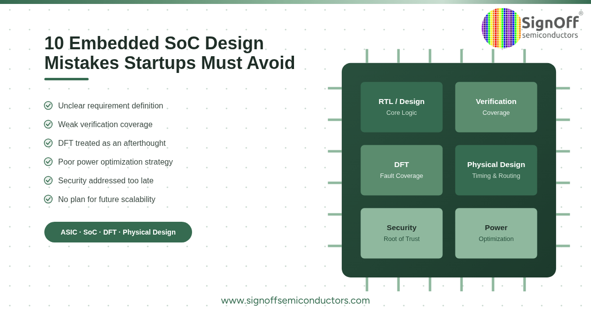
RTL development translates architectural intent into synthesizable hardware. Verification — often the most underestimated phase — must exhaustively validate functionality before a single mask is cut, because discovering a functional error post-fabrication is orders of magnitude more expensive than finding it in simulation. Logic synthesis maps RTL to a target technology library. And then physical design begins — where architecture meets physics.
Physical design is not a mechanical step. Floorplanning, placement, clock tree synthesis, routing, and signoff are deeply interdependent. An optimization made for timing closure can worsen congestion.
An improvement in power can create IR drop issues. A routing decision that resolves one DRC violation can introduce another. At advanced process nodes — 22nm FD-SOI, 28nm, 40nm — these interactions become increasingly complex, and every stage requires both tool expertise and engineering judgement.
The signoff checklist at tapeout — timing across all corners, signal integrity, power integrity, electromigration, IR drop, DRC, LVS — is not a formality. It is the collective proof that the chip will function correctly under real-world conditions: temperature variation, voltage fluctuation, manufacturing spread, and long-term reliability.
Modern EDA tools increasingly incorporate AI to assist with congestion prediction, timing path identification, and ECO recommendation. These capabilities genuinely accelerate the flow. But they amplify the capability of experienced engineers — they do not replace the judgement that experienced engineers bring.
First-time silicon programs frequently underestimate the depth of expertise that physical design and signoff require. The cost of that underestimation shows up in schedule overruns, respins, and chips that tape out but do not meet specifications.
Tapeout Is the Beginning, Not the Finish Line
After fabrication, the work is not done.
Package assembly, board integration, firmware development, silicon validation, characterization, yield analysis, production qualification, and customer acceptance are all still ahead. A chip that tapes out successfully can still fail commercially if it exceeds power budgets in the final product, misses manufacturing cost targets, or arrives too late for the market window it was designed for.
This is the part of the silicon journey that is least discussed and most consequential.
The AI companies that build successful silicon programmes are not just good at chip design. They are good at managing the complete arc from business case through volume production — treating semiconductor development as an end-to-end product strategy rather than an engineering exercise with a tapeout deadline.
A Practical Framework for AI Startups Evaluating Custom Silicon
Based on what we see consistently across programmes:
1. Wait for workload stabilization — not as a rigid rule, but as a signal. When your model changes less than your cost structure demands, it is time to evaluate silicon.
2. Define the economic objective first — cost per inference, power per device, latency requirement, or manufacturing cost target. Let the objective shape the architecture, not the other way around.
3. Profile before you architect — understand whether you are compute-bound or memory-bound, what precision is acceptable, and what the data movement pattern looks like across your full pipeline.
4. Treat physical design as a strategic capability — not a commodity. The implementation team that understands your workload will deliver better silicon than one that simply executes a flow.
5. Plan for post-tapeout — validation, characterization, and production bring-up take time and expertise that should be factored into the programme from day one.
How SignOff Supports AI Silicon Programmes
At SignOff Semiconductors, we work with AI companies across the complete arc of this journey — from the earliest conversations about workload characterization and architecture feasibility through RTL-to-GDSII implementation, physical design, timing closure, and tapeout.
We understand that every AI workload presents unique challenges, and that the difference between a successful tapeout and a costly respin often comes down to how rigorously the programme was set up before implementation began.
If you are an AI company evaluating custom silicon — whether for a first-generation accelerator or a production SoC — we would welcome the conversation.
Contact us: sales@signoffsemi.com www.signoffsemiconductors.com
SignOff Semiconductors provides full turnkey ASIC and SoC design services — RTL to GDSII — with deep expertise across physical design, timing closure, verification, and advanced-node signoff.
Comments are closed.