PD Flow II – Placement & Optimization
In last session, we discussed floor-plan & guidelines to come up with a good floor-plan. Today we discuss placement & different optimization techniques.
We hope these sessions & blogs are helping you to understand physical design concepts. Please send your suggestions / feedbacks to ‘trainings@signoffsemi.com’
Placement
In this stage, all the standard cells are placed in the design (size, shape & macro-placement is done in floor-plan). Placement will be driven by different criteria like timing driven, congestion driven, power optimization etc. Timing & Routing convergence depends a lot on quality of placement. Different tasks in placement are listed below;
- Pre-placement
- Initial placement (Coarse placement)
- Legalizations
- Removing existing buffer trees
- High Fan-out Net Synthesis (HFNS)
- Iterations of timing/power optimizations [cell sizing, moving, net spitting, gate cloning, buffer insertion, area recovery]
- Area recovery
- Scan-chain re-ordering
- TIE cell insertions
Goals of placement
- Timing, Power and Area optimizations
- Routable design (minimal global & local congestion)
- No/minimal cell density, pin density & congestion hot-spots
- Minimal timing DRCs
Before starting the placement optimization, it’s always good practice to do some analyses & checks on the design & tool settings. This would definitely help in design converge & reduce iterations.
Things to be checked before placement
- Check for any missing / extra placement & routing blockages
- Don’t use cell list & whether it is properly applied in the tool
- Don’t touch on cells & nets (make sure that, these are applied)
- Better to have limit the local density (Otherwise local congestion can create issue in routing / eco stages)
- Understand all optimization options & placement switches set in the tool
- There should not be any high WNS timing violations
- Make sure that clock is set to ideal network
- Take care of integration guidelines of any special IPs (These won’t be reported in any of the checks). Have custom scripts to check these guidelines
- Fix all the hard macros & pre-placed cells
- Check the pin access
Pre-placement
- Spare cell insertion / Metal ECO-able cells
- Magnet placement (IOs / any other interface)
- Custom / manual placement of special cells (very specific to design)
- Insertion of De-Caps (Not everyone follows this)
- Antenna diodes & buffers on block level ports
HFNS
All high fan-out nets will be synthesized (buffer tree) except clock nets & nets with don’t touch attribute. Scan-enable and reset are few examples of high fan-out nets. HFNS honors max fan-out setting.
Different Timing optimization techniques
Timing converge is one of key task in placement optimization. If timing QoR is bad, then placement cannot be qualified. Bad timing QoR at placement stage would create difficulties in timing convergence in further stages.
- Assigning more weight to critical group path
- Timing driven placement– high effort
- Allowing LVT cells for optimizations (<5% of low / ultra low VT cells)
In most of the designs only 15-25% of the paths will be timing critical. So giving more weight to these critical paths during optimization will aid in optimizing critical path delays. This can be achieved by creating group paths and assigning more weight to the critical paths.
If design is timing critical, then timing driven-placement strategy has to chosen with high effort of optimization (trade-off with runtime). But timing-driven placement is some design can create local congestion hot-spots & also global congestion will increase. Cell-padding, density screens, partial blockages and bounds can be used to reduce/fix these congestion issues.
Controlled usage of low-VT cells will help in optimizing timing critical paths. Most of the PnR tools have the option to control VT usage.
Congestion reduction techniques
- Cell padding
- Use of density screens, placement blockages
- Congestion driven placement (with high effort @ cost of runtime)
Congestion is one the major challenge in PNR of high/medium utilization designs. Placement is first & key step where congestion analysis begins & it should be under control. Both global & local congestion should be minimal with no local hotspots. A though analyses of congestion map, cell density map & pin density will be help in deciding the quality of placement.
Local congested hot-spots are very common in timing critical, high utilization designs. Cluster of AOI/OAI (Boolean function cells) / any high pin density cells will cause local hot-spots.
Power Optimization
Nowadays most of the designs are targeted to achieve less power consumption. It’s because of growing demand of hand-held battery operated devices (smart phones, tabs) & IOT. So we should keep an eye on static & dynamic power dissipation and make effort to reduce power dissipation.
Dynamic power:
Transition & Load capacitance are the two key parameters which can be controlled in placement stage to get optimum dynamic power. Iteration can be performed to arrive at optimum max transition & max capacitance. Most of the tools have option to optimize the power.
Dynamic power dissipation is directly proportional to toggle rate (switching activity). So to get maximum benefit power optimization should be done on nets with high toggle rate. ‘Low power placement’ helps to identify the net/cells with high toggle rates & load capacitance (wire length) is optimized (reduced) to reduce power dissipation.
Leakage power:
High VT & Regular VT cells will have less leakage power compared to low & ultra low VT cells. So it’s good idea to block / allow partial usage of low & ultra VT cells.
Scan chain Re-Ordering
DFT tool flow makes a list of all the scan-able flops in the design, and sorts them based on their hierarchy and perform scan stitching (clock domains, maximum chain length constraints will be considered). Scan-chain at this stage will not be layout friendly.
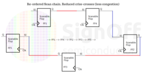
In APR tool scan chains are reordered on the basis of placement of flops & Q-SI routing. This is nothing but scan-chain reordering. Scan-chain reordering helps to;
- Reduce congestion, Total wire-length
- Require fewer repeaters in Q-SI path
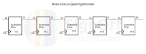
Below diagram shows pre-layout scan-chain stitched based on the hierarchy.
If scan chain reordering is not done, congestion & net/wire length will increase. Below diagram shows details:

Same flop placement with scan-chain reordered has better congestion & wire / net lengths are reduced. Refer below diagram:
What if the design has different power domains?
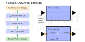
Placement flow is almost same. But in case of Abutted voltage area designs, an extra stage “Voltage Area Feed-through” is required, before placement stage.
Following tasks are done in VA-FT stage:
- Enabling VA-FT creation in tool flow
- Quick placement of the design (Requirement of VA-FT will known only after placement of all standard cells)
- Global route (To identify where all VA-FTs are required)
- VA-FT creation
- Disable VA-FT
- Continue with place & optimizations
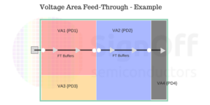
An example of FT port creation & FT buffer addition through different voltage areas (power domains) is shown in below diagram;
How to qualify placement
- Logical equivalence check & low power checks
- Check legalization
- Check PG connections of all the cells
- Check congestion, place density & pin density maps. All these should be under control
- Timing QoR / Convergence. There should not be any high WNS violations & TNS, NVP must be under control
- Minimal max tran & max cap violations
- Check whether all don’t touch cells & nets are preserved
- Check for don’t use cells (Should be Zero/ same as post Syn)
Comments are closed.
