PD Flow I – Floorplan
Physical design is process of transforming netlist into layout which is manufacture-able [GDS]. Physical design process is often referred as PnR (Place and Route) / APR (Automatic Place & Route). Main steps in physical design are placement of all logical cells, clock tree synthesis & routing. During this process of physical design timing, power, design & technology constraints have to be met. Further design might require being optimized w.r.t area, power and performance.
General Physical Design Flow is shown below,
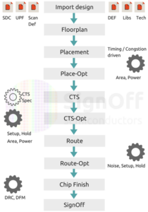
1. IMPORT DESIGN / NETLISTIN
Import design is the first step in Physical Design. In this stage all required inputs & required references are read into the tool. And also basic checks are done (design, technology consistency).
Inputs required
- Gate level netlist
- Logical (Timing) & Physical views of standard cells & all other IPs used in the design
- Timing constraints (SDC)
- Power Intent (UPF / CPF)
- FP DEF & Scan DEF
- Technology file
- RC Co-efficient files
How to qualify Import Design?
- Check errors & warning while reading netlist. Understand all warnings
- Check for uniquification & empty modules
- Check errors & warning while reading timing constraints. Understand all warnings
- Check errors & warning while reading UPF/CPF. Understand all warnings
- Timing QoR (Minimal violations with fixable WNS & TNS)
- Check MV Design (Equivalent to LP checks). Fix all errors & understand all warning
- Check for assign & tri statements (Usually its checked & fixed after Synthesis)
Timing analyses after Import Design
It is always a good practice to do quick timing analyses after import design. Even though post synthesis timing analyses is done in timing tool (PT, Tempus/ETS), it’s better to check post synthesis timing QoR in PnR tools also (ICC, Innovus, Olympus) before actual implementation starts.
Why it is required?
ICC/Innovus optimizes critical timing paths (violating paths) which are seen by it. There can be chances that PnR tool is showing a complete different timing QoR (huge violations) compared to Post Syn QoR seen in PT/Tempus. It can be because of correlation issue / constraints issue. We can avoid unnecessary optimization; timing & design closure will be easy if we correlate Import Design timing QoR with Post Syn timing QoR.
2. FLOORPLAN
Floorplan is one the critical & important step in Physical design. Quality of your Chip / Design implementation depends on how good is the Floorplan. A good floorplan can be make implementation process (place, cts, route & timing closure) cake walk. On similar lines a bad floorplan can create all kind issues in the design (congestion, timing, noise, ir, routing issues). A bad floorplan will blow up the area, power & affects reliability, life of the IC and also it can increase overall IC cost (more effort to closure, more LVTs/ULVTs)
Before staring of Floorplan, it is better to have basic design understanding, data flow of the design, integration guidelines of any special analog hard IPs in the design. And for block/partition level designs understanding the placement & IO interactions of the block in Full chip will help in coming up with good floorplan.
What is required to come with a good floorplan?
- Basic design understating
- Data flow diagram (DFA / Analyze logic connectivity in Synopsys ICC)
- Integration guidelines
- IO / Pin placement requirements
- Special requirements from Full Chip floorplan
- MV / LP requirements. Understanding of PDs & Vas
Different types of partitions / blocks
- Memory intensive digital cores, graphic cores
- Partitions / Blocks with analog Hard IPs
- DDR & other High Speed Interface partitions / blocks / sub-systems
- Channel partitions
Partitions with different critical tasks
- Timing critical
- Routing critical / Congestion
- Blocks with complex Clock structure
Types of floorplan techniques used in Full Chip plan
- Abutted (All inter block pin connections are done through FTs)
- Non abutted (Channel based. All inter block pin connections are routed in channels)
- Mix of both – partially abutted with some channels

FLOORPLAN STEPS
- Size & shape of the block (Usually provided by FC floorplan)
- Voltage area creation (Power domains)
- IO placement
- Creating standard cell rows
- Macro-placement
- Adding routing & placement blockages (as required)
- Adding power switches (Daisy chain)
- Creating Power Mesh
- Adding physical cells (Well taps, End Caps etc)
- Placing & qualifying pushdown cells
- Creating bounds / plan groups / density screens
Detailed discussion
2. Voltage area creation
In multi-voltage & multi power domain designs, voltage areas are required to guide the tool to understand different domains.
There are two methods to create voltage area;
- Abutted voltage area (Cells are not allowed to place in default voltage area)
- As is no default domain area, voltage area feed-through (VA-FT) are required to cross over different voltage areas.
- Non-abutted voltage area (Cells are allowed to place in default voltage area)

1. Shape & size of the block / partition
In most of the case, block size & shape is decided by FC floorplan. Rectangle/Square shape is best in terms of floorplan & further design closure. But in many case, floorplan can be of rectilinear shape with many notches. It is always good practice to discuss with FC floorplan team for any scope to improve block/partition level floorplan.
3. IO / Pin placement
IOs / Pins are placed at the boundary of the block. Usually pin placement information is pushed down from FC floorplan. But these locations can be changed based on block critical requirements. Any change in pin location has to be discussed with FC floorplan team. Timing critical interfaces need special attention, like next 2-3 levels of logic from IOs are pre-placed near the IOs). Source synchronous interfaces requires delay balancing taking OCV into considerations (This will require manual placement & scripting)
4. Row creation
Rows area created in the design using cell-site (unit / basic). Rows aid in systematic placement of standard cells. And standard cell power routes done considering rows.

Rows can be cut, wherever cell placement is not allowed OR hard placement blockage can also be used.
5. Macro placement
Step 1 – Understand Pins & Orientation requirements of Macros

Step 2 – Follow data flow / hierarchy to place the Macros. Make use of reference floorplan if available
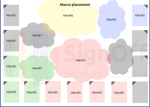
Step 3 – All the pins of the Macros should point towards the core logic
Step 4 – Channels b/w macros should be big enough to accommodate all routing reqs & should get a minimum of one pair VDD & VSS power grids in the channel

Automatic Floorplan / Macro-placement
Most of the PnR tools provide automatic floorplan option. Automatic floorplan option creates its own macro placement based on the effort & other options. But these options are not matured enough to give optimum floorplan for all kind of designs. This option will be handy, when design has 100s of Macros, but generated floorplan needs lot of modification for further optimizations.
How to qualify Macro – Placement
- All macros should be placed at the boundary
- Check the orientation & pin directions of all macros
- Spacing b/w macros should be enough for routing & power grid
- Macros should not block partition level pins
- [Iterations] Less congestion & good timing QoR – These cannot be achieved in one shot, but need few iterations [Thorough & deep analyses are the key things while iterating]
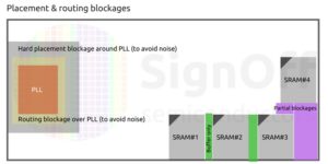
6. Adding placement & routing blockages
Buffer only blockages are added in channels b/w macros. Partial placement blockages can be added b/w the channels blocking sequential cells (whose placement in channels can degrade CTS QoR). Partial blockages are added in congestion prone areas/notches/corners
7. Adding power switches
Power switches are required to gate the power supply of gated domain when not required. Power switches are MT-CMOS (multi-threshold) cells, which will have very high threshold voltage when device is OFF & very low threshold voltage when device is on.
Power switches are inserted in power mesh & supply to all gated domain cells will be through power switches. Hence a single / few switches are not enough. A strong network of power switches connected in daisy chain fashion will be inserted in the design.

8. Adding special cells (Well Taps, EndCaps, Spare Cells, Metal ECO-able cells etc)
Well connection – Almost all standard cell libraries are tap-less (substrate connections are not done @ cell level). So Well-taps cells are added in partition/chip level to tie the wells to VDD/VSS. Tap-gate spacing has to be met while adding well-tap array.


EndCap Cells – These cells are inserted to take care of boundary DRC of Wells & Other layers. End Cap Cells ensure proper terminations of rows, so that no DRC are created. This is a physical-only cell.
How to qualify Floorplan?
- Check PG connections (For macros & pre-placed cells only)
- LP / MV checks on floorplan database
- Check the power connections to all Macros, specially analog/special macros if any
- All the macros should be placed at the boundary
- There should not be any notches / thin channels. If unavoidable, proper blockages has to be added
- Remove all unnecessary placement blockages & routing blockages (which might be put during floor-plan & pre-placing)
- Check power connection to power switches
- Check power mesh in different voltage area voltage area
- Check pin-layers & check layer directions (H-V-H)
Comments are closed.
